Quantcast
Channel: Francoise in 3D Archives - 3D InCites
Viewing all 256 articles
Browse latest View live

With the Potential to Save Lives, Smart Rock Bolt Takes Home the IPSO CHALLENGE 2015 Grand Prize

$
0
0

Now in its third year, the IPSO CHALLENGE 2015, an annual event run by the IPSO Alliance, requires entrants to showcase how they use Internet Protocol (IP) and open standards in building devices for the the Internet of Things (IoT). This year’s entries came from around the world in a wide range of industry categories. Semi-finalists ranged from IoT platforms to a host of smart objects. Up against some tough competition, the Smart Rock Bolt emerged victorious, winning the grand prize of USD $10,000 during a ceremony held a the Designers of Things Conference, December 2, 2015 in San Jose.

Developed by Luleå University of Technology (LTU) and Eistec AB, the Smart Rock Bolt is a vibration-sensor-based device that has the potential to save miners lives by instrumenting tunnels to detect potential catastrophic collapses. 3D InCites spoke with Jens Eliasson, associate professor at LTU, and to Pete St. Pierre, president, IPSO Alliance Board of Directors, to learn more about this device, and what set it apart from its competitors.

The idea for the Smart Rock Bolt came to Eliasson as he contemplated the challenges and dangers faced by Sweden’s mining industry. Rock bolts are used to secure tunnels and other underground cavities, which can become unstable from blasting and other mining activities that cause movement and cracks within the rock walls, and ultimately result in tunnel collapse, he explained. Too much movement can damage these bolts, but it’s almost impossible to evaluate a bolt’s integrity as 95% of it is embedded inside the tunnel wall. Eliasson turned to the IoT to solve the problem. By embedding sensors that measure force load and monitor seismic activity using vibration sensors, it’s possible to keep track of vibrations and tell if a bolt has been torn in two. Add on-board signal processing to transmit information to gateways, which in turn propagates the information to control systems, and it’s now possible to perform real-time monitoring simultaneously on many rock bolts, and potentially prevent these tunnel collapses from occurring.

Eliasson explained that by basing all the communication on IP and IPSO Object Models to express functionality for each bolt, they were able to create plug-and-play devices that automatically register with a gateway to monitor and control systems. “The power of using standards is that it gives us the opportunity to add incremental value to the bolts by updating and adding sensors that, for example, could detect fire in a tunnel,” he said, adding that the standards also make the technology bolt agnostic.

Thanks to the IPSO Object Models, the technology is extendable beyond the mining industry to address similar dangers on bridges, auto and train tunnels, freeway slopes, and even underground rail systems. Additionally, the vehicle for the sensor technology doesn’t need to be a bolt – it could be embedded in any object used to secure structures, such as load beams on houses. Really, the possibilities are endless. It’s this extendibility that set the Smart Rock Bolt apart from the other entrants to win the IPSO CHALLENGE.

St Pierre noted that the range of entrants this year was “all over the place” from platform solutions targeted at developers, to objects, like the Smart Bolt, implementing intelligence to solve real problems. He also said that this year’s entries were up against the most refined set of solutions in three years of the IPSO CHALLENGE. “The open standards are solid enough, it’s easy to pick them up. So IPSO shifted focus from why to use the IP to how to get it done,” he explained.

The toughest competition for the Smart Bolt were the two-runners up, said St. Pierre, as they also created devices comprising a network of sensors talking to each other to solve a real-world problem. Second place went to EISOX’s Intelligent Thermostatic Radiator Valve, “a smart heating regulation system that autonomously controls the temperature inside each room of a house depending on human behavior, by using artificial intelligence algorithms and highly efficient human presence sensors.” This device is European market focused, as that’s where these types of radiators are used most. Third place went to MicroPnP’s IoT platform, a “a zero-configuration Internet of Things platform that instantly connects your things to the cloud.” A fourth IPSO CHALLENGE semi-finalist, Heads Up! received the People’s Choice Award. This device uses a smart object equipped with an accelerometer to monitor the position of a patient’s head when recovering from pneumatic retinopexy surgery, a procedure used to heal retinal detachment.

The winner of the IPSO CHALLENGE was chosen based on the use of open standards; and use of IP in an open manner, with as few proprietary elements as possible, so more can be used together. The fact that Smart Bolt also used IPSO Object Models may have been the tipping point, noted St. Pierre, at least from his perspective. “Along with the marketability and viability of the product, its not just about ‘have I solved the problem today with todays technology.’ Clearly they had a vision for additional sensors to add and what the utility is. They came up with a practical result that creates real business opportunities for them or for partners,” explained St. Pierre.

So what plans does Eliasson have for the $10,000 prize money? “We will create a spinoff company from the research institute, team up with mining companies and take this technology all the way,” he said. “We hope to be installing 10 devices in June.”

3D InCites congratulates winners and runners-up of this year’s IPSO CHALLENGE, and we applaud your ingenuity. Let’s see what you’ve got up your sleeves for next year. ~ F.v.T

The post With the Potential to Save Lives, Smart Rock Bolt Takes Home the IPSO CHALLENGE 2015 Grand Prize appeared first on 3D InCites.
Happy Holidays, from your friends at 3D InCites!

$
0
0


The post Happy Holidays, from your friends at 3D InCites! appeared first on 3D InCites.

At 3D ASIP 2015, Variety is the Spice of Life

$
0
0

Staying relevant in the ever-expanding technology landscape that is the semiconductor packaging industry can be a struggle for an event that’s been laser-focused on one emerging segment since its inception. But this past week, 3D Architectures for Semiconductor Integration and Packaging  (3D ASIP 2015) delivered a program that not only addressed the progress of 3D integration, it also expanded the conversation to include other developments in high-density advanced packaging (HDAP), and heterogeneous system integration.

While previous editions of this event focused primarily on processes and technologies for through silicon via (TSV) fabrication  and subsequent backside processing steps for interposer and 3DIC devices, as the technology reaches maturation, attention has shifted to what products are implementing 3D, and how do we address power, performance, area, and cost (PPAC) for consumer electronics applications. Essentially,

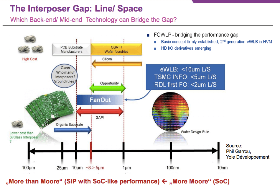
As Thibault Buisson, Yole Developpement explained during his plenary talk, Comparison of New Memory Architectures, continued scaling is widening the disparity between printed circuit board (PCB) feature sizes, and CMOS feature sizes. 3D TSV and fan-out wafer level packaging (FOWLP) are filling this gap (FIgure 1). As predicted for years, the memory market is emerging as the next bastion of TSV growth and adoption. Indeed, 2015 will go down as the year of 3D TSV stacked memory.

3D ASIP copy

According to Buisson, graphics cards have been first application to use 3D stacked memory. Additionally, he says many leading OEMS plan to release new products using HBM and hybrid memory cube (HMC) memories targeting HPC applications like networks, routers, and switches. Additionally, Toshiba has implemented TSVs in its 3D NAND. Furthermore, new products will be Si-interposer based, or directly integrated on the PCB, and could contain multiple ASICs and multiple memory cubes.

Presentations by Minsuk Suh, SK Hynix; Kazuyuki Higashi, Toshiba; Tom Gregorich, Micron; and Bob Patti, Tezzaron Semiconductor, further drove home the availability of a plethora of 3D DRAM technologies implementing TSVs, and the reasons why.

Suh noted that HBM has overcome all the DRAM challenges for high bandwidth memory. While TSVs are still an expensive technology, he says they are already in mass production in high-end applications, which will help decrease the cost.

One of the year’s biggest success stories that implemented HBM and interposer technology is AMD’s Radeon Fury, which has been making headlines as the first implementation of 3D High Bandwidth Memory (HBM) integrated into the Fiji GPU. Bryan Black presented a talk, The Road to The Fiji GPU”, offering an inside look at all that was involved to get there. “Now that we’ve done the Fiji Chip – we’ve figured out how to do this, and we can do it in anything,” he said.

Calling TSVs ‘the most promising technology for future” Toshiba’s Higashi noted that in comparison to wire bond, TSVs offer 10X the inter-chip connections at <1/10th parasitic capacitance to achieve high speed and low power. Moreover, Toshiba has adopted a backside via process for its TSV NAND because they believe it to be a lower cost approach than via-mid, because it requires fewer process steps.

Gregorich noted that while there’s consensus that the 3Di TSV DRAM cube is a good idea and is demonstrating good yields in different high performance computing applications, the solution for consumer products may be different because each segment (PC, tablet, phone, wearable) has unique requirements (ie: density, bandwidth, form factor, power usage, power handling, low cost). “While solutions for the consumer markets might be based on 3D TSV DRAM cubes, the interface between the DRAM and the CPU is the key to providing low-cost, high bandwidth, and low power,” he said. “The challenge is how to adapt it into other markets.” The smartphone, for example, is very dependent on package-on-package (PoP) structure. How do we adapt the PoP to wide interface so we can continue with that structure but still put TSVs in it.

Figure 2: The right I/O for every need.

Figure 2: The right I/O for every need.

According to Patti, we will see revolutionary changes over the entire market in the next 3-5 years, and the future is definitely about More than Moore. “How do we put all these things together? We’ll have a super computer the size of a softball,” he said. At Tezzaron, the focus is not only on storage-class memory, but on integration of different functional layers that Patti breaks down into memory bit layer, controller layer, and I/O layer. The I/O layer could be Pico-SerDes, SerDes, or photonics; whichever is needed (Figure 2). This is stacked on a Si or organic interposer, based on density requirments. Tezzaron has the foundry platform to support all of this.

Let’s remember that 3D TSVs are only one option in the HDAP wheelhouse. While we are told cost will come down naturally as 3D TSV volumes in high performance computing applications take hold, research and development on other high-density approaches didn’t come to a screeching halt while we were trying to solve issues with TSVs. Ultimately, it’s not an “us vs. them” conversation. It’s a “which technology is the best suited to the job at hand” conversation. Brandon Prior, Prismark Partners, pointed out that adoption of 3D integration doesn’t just require process technology to be there, but also requires alignment of image sensor, logic, and memory die size to be cost effective.

Prior also noted that Intel and Samsung remain skeptical of FO-WLP. At this time, neither have plans to install fan out capacity, and it’s not seen as cost-effective means to make a thinner package. However, the expectation that Apple will proceed with TSMC’s integrated fan-out (InFO FO-WLP) for the A10 processor in 2016 is enough to make other major industry players like SPIL/Xilinx, Amkor, Deca, and many others step up their offerings in the HDAP space.

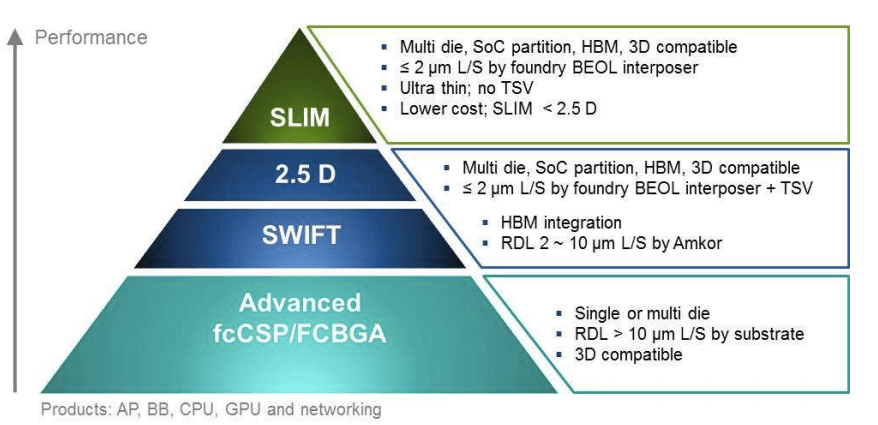
One thing was made clear through three days of presentations — varied options are not in short supply. In addition to TSMC’s KC Yee, who espoused the benefits of TSMC’s InFO technology, we also heard from Dyi-Chung Hu, of Unimicron, who introduced embedded high-density film (eHDF), a high-density substrate platform that eliminates the need for TSVs (he called them TXVs), Si interposers, and underfill. And we heard from Xilinx Fellow, Suresh Ramalingam, who talked about the company’s silicon-less interconnect technology (SLIT), which also eliminates the need for TSVs. Lastly, Amkor’s Mike Kelly talked about the company’s many options to address line/space requirements at different sizes to address the gap between 1µm and 8µm l/s from it’s most advanced technology, silicon-less interposer module (SLIM) that doesn’t use TSVs; to the now conventional 2.5D/3D solutions to silicon wafer integrated fan-out (SWIFT), to address 2-10µm l/S.

amkorFC copy

Figure 1: Amkor’s advanced flip chip product positioning.

Differentiating between all these HDAP offerings that are suddenly available is a daunting task. But as Yee noted in his presentation, the more options available to the customer, the better. Perhaps it’s time to lose the 3D and rename this conference, High-Density Architectures for System In Packaging? Ah yes – and we didn’t even touch on the heterogeneous integration portion of the event. Yet. More to come! ~ FvT.

The post At 3D ASIP 2015, Variety is the Spice of Life appeared first on 3D InCites.
3D ASIP 2015: 3D Manufacturing Processes from the Early Days to the Present

$
0
0

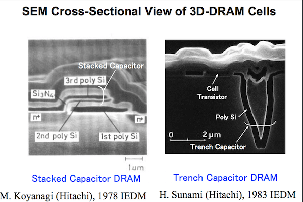
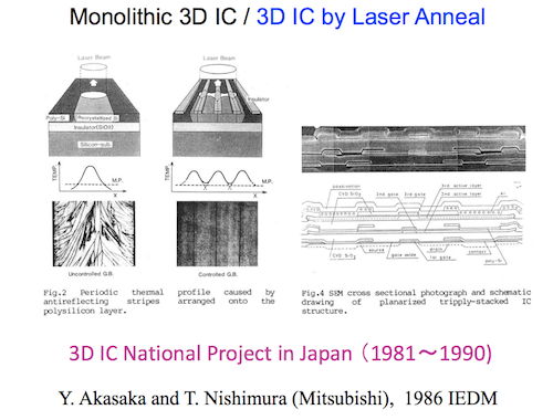
For the first time since the 3D Architectures for Semiconductor Integration and Packaging (3DASIP) Conference was established, the organizing committee decided to acknowledge the work of two researchers who were instrumental in developing the core processes that enabled 3D TSV development. In a brief ceremony, Dr. Phil Garrou presented 3DIC Pioneer Awards to Professor Mitsumasa Koyanagi, Tohoku University and Dr. Peter Ramm, Head of Department Heterogeneous System Integration, Fraunhofer EMFT “for their pioneering work in the 1990s in the area of chip stacking with TSV thinning and bonding, which lead to today’s 3D DRAM stacking and high-density silicon interposer technologies. Our industry thanks these pioneers for their foresight and their persistent efforts to bring these technologies to commercialization.” Each recipient provided the attendees with a trip down 3D memory lane through presentations of their work in this field as far back as 1985, which is when Professor Koyanagi started working on 3D versions of DRAM. I had no idea we had been working on this for so long.

I was most intrigued by some of the earliest images Koyanagi shared. The first is early SEM images of what would later become Through Silicon Vias (TSVS). The second diagrams monolithic 3D IC concepts that he worked on between 1981 and 1990. “Perseverance” doesn’t begin to describe the efforts here.

koyanagi1

koyonagi2


The history of 3D IC work at Fraunhofer Munich started in 1987, as part of various German and European Research Projects with ongoing support provided by Siemens and Infineon that occurred between 1987-1989, 1993-1996; 1993-2003, and now from 2007continuing through 2017. That’s 30 years devoted to developing processes for:

  • 3D CMOS Devices
  • Performance and thermal issues of 3D-ICs
  • TSV processes
  • Wafer thinning & thin die handling
  • Wafer bonding
  • Die-to-wafer stacking technologies (KGD)
  • 3D integration technology is now entering a mainstream
  • Memory stacks, memory/logic, … (high density TSVs)
  • Heterogeneous sensor/IC integration (medium density TSVs)
  • Choice of 3D process depends on
  • Performance, TSV/pad pitch requirements
  • Reliability requirements

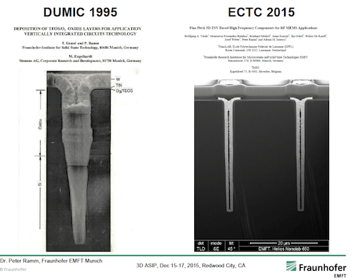
Ramm said ongoing work is focused on TSV based RF-MEMS & RF-IC and highly reliable, ultra-low power 3D heterogeneous MEMS/IC systems. This image aptly illustrates what 10 years of work achieved in developing and fine-tuning processes for TSVs.

ramm1 copy

Understanding how much time and effort has gone into developing 3D processes that are appearing in products today makes commercialization of 3D TSVs that much more impressive. And we’re not done yet, as evidenced by presentations from several equipment suppliers on their continued efforts to further optimize processes to improve performance and reduce cost.

Day One of the conference featured a half-day tutorial on temporary bond/debond processes from research institutes, RTI International and CEA Leti; materials vendors HD Microsystems and Brewer Science; and equipment manufacturers, EV Group, TOK, and SUSS MicroTec.

I caught 3 of the six presentations, and got the distinct impression that the industry hasn’t completely figured this out yet. Or rather they have, but as Molly Hladik, Principal Applications Engineer, Brewer Science, explained to me, there’s not a one-size–fits-all solution. There are many and varied requirements depending on the application, and so what combination of material, process, and equipment suits one application may not suit another.

For example, from the materials menu, there’s a choice between thermoplastic, thermosetting, photosetting, and combinations. There’s also device-side release layer, or carrier side release layer materials to consider. For debonding, there’s mechanical debond, and laser-assist. Then there’s the matter of residue cleaning, and dicing tape. To complicate matters further, which process to choose depends on whether your process flow is for fan-out wafer level packaging (FOWLP), interposer integration, or 3D IC stacks for memory.

The tools must be configurable to a multitude of processes and material properties, and that’s a huge challenge. Not only that, but manufacturers must make all of these available to their customers. The good news is, all these equipment and materials vendors are reporting good yields when the right process is selected for the right application. It’s just a matter of knowing which combination suits your application, and which manufacturer has the capacity to deliver.

In one session devoted to equipment and metrology, there were three more process-focuses presentations by Markus Wimplinger, EV Group; David Butler, SPTS; and Rajiv Roy, Rudolph Technologies. (a fourth by Prashant Aji, KLA Tencor, was cancelled).

Wimplinger talked about permanent bonding for 3D ICs in high volume manufacturing. He said the main battles of taking wafer-to-wafer bonding to HVM have been alignment accuracy and throughput. Carefully controlled plasma activation is critical to the process.

Wimplinger focused on hybrid bonding, which bonds metal to a dielectric layer at room temperature, and is a preferred method for W2W bonding, as it is low cost and high-density solution. He gave a nod to Ziptronix as pioneers in the hybrid bonding space for its direct bond interconnect process (DBI).

According to Wimplinger, second-generation 3D backside illuminated (BSI) CMOS image sensors (CIS) use hybrid bonding without TSVs to form connections in the bonding interface. “Wafer bonding has arrived at the point in high accuracy and alignment where it enables high density interconnects, and is bringing 3D to the consumer market,” said Wimplinger.

David Butler, SPTS, stepped outside the company’s usual topic area of TSV etch process optimization to present a new process used for both FOWLP and 3D integration – plasma dicing. “We’ve heard a lot about large die today (700mm), but there’s far more being made with tiny die,” he said. Plasma dicing is driven by the need for more die, smaller die and smaller, thinner packages. It can reduce the widths between die, allowing for up to 80% more die per wafer.

Traditionally, dicing is done using a mechanical dicing saw. Alternatively, plasma dicing is a chemical process that is non-damaging, and results in stronger die post-separation. Butler said it doesn’t required water, there is no vibration, and there is no debris. He also said that process control via end point detection and notch prevention is critical to successful plasma dicing, and is something SPTS’s system can do.

Lastly, Roy talked about Rudolph Technologies latest advancements in lithography, inspection, and software to address the need for finer line/space requirements coming with high density FOWLP. Two areas affecting final yield has been die shift and wafer warpage. The company has developed lithography processes to correct both. They’ve also introduced an industry first: high-speed fluorescent imaging for semiconductors. Roy explained that the variety of materials used in FOWLP requires more than just bright field imaging to detect possible defects. They’ve discovered that by combining fluorescent and bright field imaging, they can detect more residues.

With FOWLP and 3D ICs becoming commercialized and approach volume manufacturing, it’s clearly worth the effort to continue to improve processes to increase yields and ultimately lower costs.  ~ F.v.T.

The post 3D ASIP 2015: 3D Manufacturing Processes from the Early Days to the Present appeared first on 3D InCites.
The European 3D Summit: From Roadmaps to Reality

$
0
0

In its fourth edition and with a new name, the European 3D Summit (formerly the European 3D TSV Summit) reflected the shift from R&D to the real business of 3D integration and advanced packaging, and highlighted the significant growth this market space has undergone in the past year. It has also taken a new perspective, as we no longer view fan-out wafer level packaging (FOLWP) and 3D through silicon via (3DTSV) stacks as competitive technologies, and therefore adversaries; but as two classes of solutions that provide options to serve varied performance requirements at the lowest possible cost. Ultimately, his year’s event was all about the advanced packaging sector, in all its dimensions, as finally being acknowledged for the value it brings to the table. (Even Intel is acknowledging that multi-chip packaging is necessary to reach really high speed I/Os – as they announced at ISS that they will be starting to implement 2.5D and 3D packaging into processors this year).

In the early days of the march to 3D integration, this conference was more academic. Now, it has evolved into a business-focused conference as processes matured and are being integrated into products. Whereas we got used to seeing technology updates from a similar group of presenters and/or companies, this year there were only a few repeat presenters, and many new product-focused presentations on 3D integration for high performance computing products, imaging products, wearables, medical, MEMS integration, and more.

In addition to the market updates, which I will cover in more detail in a subsequent post, there was lots of discussion about 3D system-level integration, what’s driving it, and how it implements the whole spectrum of interconnect technologies including wire bond, flip chip, redistribution layers (RDL) and TSVs. Additionally, there were more references than ever before about advanced hybrid bonding, including Ziptronix’ DBI and DBI-like approaches being implemented into BSI 3D stacking, in addition to wafer-to-wafer and die-to-wafer bonding.

What wasn’t discussed at this conference was as notable as what was discussed.

Glass interposers, which in the past had merited its own session, came up only in passing, such as in the X-Fab presentation, because the company offers through glass vias (TGV);  and briefly as part of the Yole Dévéloppement market update. Monolithic 3D IC, which has been a fairly hot topic for the past year or so since Leti introduced CoolCube, didn’t make an appearance at all. There was no discussion of test, or thermal management issues, nor solutions for either. This could be because as productization takes place, these issues have been solved by manufactures and have become a non-issue. Or there was nothing new to report. (Or maybe such topics just didn’t really fit into this year’s agenda, with so much other cool stuff to talk about.) And there were only two presentations devoted to design topics: Fraunhofer’s Andy Heinig stressed the need for assembly design kits (ADKs) that serve the same purpose for assembly as process design kits (PDKs) do for chip manufacturing; and Mentor Graphics’ demonstrated its experience in the chip/package/board co-design space aimed at satisfying that need.

We did revisit an old favorite with a new twist: temporary bond/debond. 3M presented new adhesives and processes they’ve been working on with SUSS MicroTec. Nanium and Amkor each talked talked about temporary bond/debond for FOWLP debond for thin wafer handling for FOWLP PoP configurations. Nanium is trading in its metal carrier for proprietary ceramic carriers for WLPoP, noted Steffen Kröhnert. This is because both glass and Si carriers don’t hold up to the debond process step due to the different properties of a reconstituted wafer. Conversely, David Hiner explained that as Amkor uses a chips-last vs. chips-first approach, the RDL is built right on the carrier, and the mold compound doesn’t come into play as part of the temporary bond/debond step.

Anne-Marie Dutron, general director of SEMI Grenoble and organizer of the event, said that expanding the focus resulted in more attendees, as well as from different sectors of the market. I weighed in with some of the attendees to get some additional feedback on the event and gain some insight from their perspective.

Even with the varied topics, Thomas Fries, FRT, commented that there was some redundancy throughout the presentations – for example with the multiple use of Phil Garrou’s now famous “mind the gap” slide (Figure 1). However, Fries noted that this wasn’t necessarily a bad thing; it’s an indication that we are approaching the mainstream with technology. Rather than technically detailed, there was more of a “mine is better than theirs” approach, as manufacturers vie for customer business. “It shows we are approaching some kind standardization in the industy,” he noted. “As a supplier of metrology solutions, this makes my life much easier.”

Figure 1: Many presenters showed this slide to demonstrate the gap FOWLP can fill.

Figure 1: Many presenters showed this slide to demonstrate the gap FOWLP can fill.

Tim Anderson, Fogale Nanotech, was a newcomer to the event, and offered some observations from that perspective. He said the presentation material was great, and overall appropriate to the topics. On the whole, as a veteran of front-end processes, he finds the whole packaging area very confusing. The terminology doesn’t truly fit what it is. The conference helped him to clarify and unscramble the scrabble board that falls under embedded packaging technologeis  – with different companies changing up the terms to reflect different approaches, for example we have  eWLB, WL-FO, SWIFT, SLIM, InFo, RCP, Chips-First, and SLIT, all variants of conventional and high density FOWLP (Figure 2).

Figure 2: This slide, presented by Steffen Kroehnert, Nanium, illustrates the variety of options being developed under the FOWLP umbrella.

Figure 2: This slide, presented by Steffen Krohnert, Nanium, illustrates the variety of embedded packaging technology options available.

For Ehrenfried Zschech, Fraunhofer IKTS, the main takeaway from the presentations of this year’s conference is that the increasing variety of 3D solutions, and therefore simultaneously the number of materials integrated in 3D stacks brings new challenges to reliability and requires study, particularly of thermal stress-induced effects.

Not long after I decided to focus on 3D packaging and start 3D InCites, it occurred to me that at some point, the third dimension would be a given in developing next-generation advanced packaging technologies. Because whether or not TSVs are involved, the third dimension certainly would be. This year’s European 3D Summit, from the name change to the content presented, was an indication to me that we are practically there.  ~ FvT

The post The European 3D Summit: From Roadmaps to Reality appeared first on 3D InCites.

European 3D Summit: Market Analysts Weigh in on FOWLP, 3D Packaging, and SiP

$
0
0

As it has in year’s past, the 2016 European 3D Summit kicked off with a market briefing. We heard from the usual suspects: Yole Dévéloppement (Rozalia Beica) and TechSearch International Inc. (Linda Bal). Additionally, in a nod to the business-centric tone of the conference, the committee invited Christian Knochenhauer, McKinsey and Company, to present on value creation in the packaging, assembly and semiconductor industry. Romain Fraux, System Plus, presented analyses of real products implementing TSV technologies, not only for the purposes of interconnect, to provide insight on the broader application of this technology.

While Knochenhauer’s presentation was rather sobering — apparently those packaging cornflakes realize higher profit margins than those packaging computer chips — It didn’t dampen the spirits of the attendees too much, as what was to follow was so much more optimistic.

Basically, according to Knochenhauer, the semiconductor industry is highly cyclical and under-performing (tell us something we didn’t already know). And only eight out of 188 firms in their database have performed consistently positive since 1996, while 115 companies have destroyed economic value. He also said there is no clear winning formula to generate value in assembly and test. Semiconductor is a winners-take-all industry (and I don’t have to list which ones are the winners.) However, he did say the smaller players in analog and capital equipment generate value by being market leaders in niche positions.

The market updates took a more upbeat turn, as Fraux, Bal, and Beica added to the growing list of real products that implement advanced wafer level packages, including FOWLP and 3D TSVs, as well as to the list of OSATS, IDMs and foundries that offer variations on FOWLP.

3D TSV in HVM
While Beica talked about the continuing trend of mergers acquisitions, she noted that 3D packaging is currently at the forefront of the semiconductor industry, as it offers faster time-to-market and allows for integration of all different functionalities in the same devices, which is difficult at advanced technology nodes, making More than Moore a more attractive option. Even the foundries are getting involved, she said. The bottom line is, the advanced packaging market is on the rise, and is currently dominated by flip-chip technologies. However,  while 3D IC and FOWLP are both currently small markets,  high growth is expected. Where there is growth, there is opportunity.

samsunghynix2

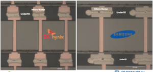
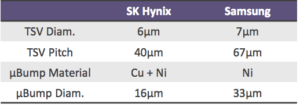
Figure 1: Comparison of SK hynix HBM and Samsung DDR4 with TSVs. (courtesy of System Plus)

Gone is the speculation for whether 3D TSVs will be realized in high volumes. In his presentation comparing 3D TSV technology trends in memory, MEMS, and sensors, Fraux revealed that the finger print sensor on the iPhone 6s contains TSVs, and are the highest volume TSVs on the market, with 50K wafers produced. Other key players, as we know, are SK Hynix, with TSV in volume production in the HBM, and Samsung with its DDR4 memory. Raux presented detailed comparisons of both processes. In summary, he noted that processes for Samsung and SK Hynix’ stacked memory devices are close and share the same cost structure (Figure 1). Additionally, Beica declared that TSVs have gone mainstream for high-end computing applications. Figure 2 shows the roadmap for TSV product implementation.

Figure 2: 2.5D/3D commercial announcements implementing TSVs. (Courtesy of Yole Dévéloppement)

FOWLP: Filling the Gap
Before diving into the FOWLP discussion, Bal talked about the increased numbers of wafer level packages (WLP) in consumer mobile products and wearable devices, driven by the desire for thinner products, as well as smaller form factor and low cost. “People think that thinner products are better, but this is a consumer perception,” she noted. “Thinner doesn’t make it work better.” Tear-downs of various smartphones resulted in an average of 5-7 WLPs per phone. WLP are also showing up in digital cameras and camcorders, laptops and tablets, medical and automotive devices, noted Bal.

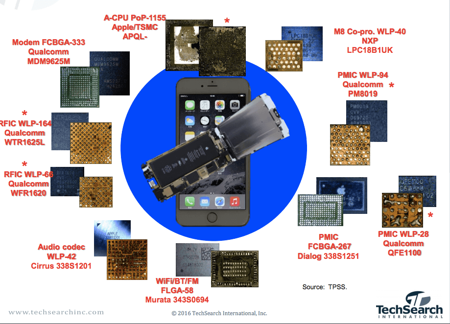
Drivers for FOWLP are similar to WLP, with the added benefits of being able to achieve finer line/space than conventional WLP, accommodate die shrinks, and allow for multi-die integration. When FOWLP is implemented in the bottom package of package-on-package (PoP) configurations, the result is a lower profile package with high routing density that enables system integration at a competitive cost. According to Bal, this is why FOWLP is being rapidly adopted into consumer mobile applications to fill the performance gap between WLP and interposer and 3D ICs (Figure 3).

Figure 3: Apple iPhone: RF, PMIC, AP Migrating to FO-WLP? (courtesy of TechSearch International, Inc)

Figure 3: Apple iPhone: RF, PMIC, AP Migrating to FO-WLP? (courtesy of TechSearch International, Inc)

Both Bal and Beica detailed OSAT activities in FOWLP, and talked about conventional approaches, alternatives to reconstituted wafer, and and new developments for high-density fan-out. They also both reported that the mobile and wireless markets are the primary markets for FOWLP, and that it’s also starting to be adopted into automotive and medical markets. For example, in automotive applications, it’s being adopted for mmWave radar for advanced driver assist systems (ADAS).

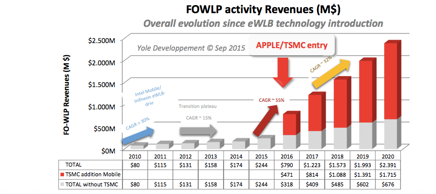
According to Beica, the entry of Apple/TSMC into the FOWLP space caused Yole to adjust its forecast of CAGR for the 2014-2016 from 15% to 55%, with and additional  jump of 32% between from 2016-2020. Additionally, Beica predict that the market for FOWLP will exceed $2B by 2020 (Figure 4). TechSearch International Inc. predicted an overall CAGR for FOWLP of 87% from 2015-2020.

Figure 4: Impact of Apple/TSMC entry into FOWLP market. (Courtesy, Yole Dévéloppement)

Figure 4: Impact of Apple/TSMC entry into FOWLP market. (Courtesy, Yole Dévéloppement)

A few Words on SiP
One of the advantages of all varied advanced WLP platforms — wirebond, FC, embedded, 2.5D and 3D — is that together, they enable system-in-package (SiP) platform. Beica defined SiP as two or more components with different functionalities packaged into a system or sub-system. She explained that SiP allows for smaller form factor, more flexibility, and more technology integrated into the same package, resulting in higher performance, faster time-to-market, lower cost, IP protection, and higher added value. It suits various markets including wireless communications, consumer, automotive, medical, and IoT. Beica noted that SiP already dominates smartphone platform, with many growth opportunities.

All in all, it seems that after years of anticipation, advanced packaging’s importance to the industry is being acknowledged. No longer is it the necessary evil – it is a value-add. This set a positive note for the remainder of the conference, and set the perfect stage for the remaining presenters to tell their stories. ~ F.v.T

The post European 3D Summit: Market Analysts Weigh in on FOWLP, 3D Packaging, and SiP appeared first on 3D InCites.
The European 3D Summit: The Gala Quiz

$
0
0

Hands-down, the best part of last week’s 2016 European 3D Summit was the Gala Dinner at the Chateau Sassenage, and in particular, the Gala Quiz. (I think my co-attendees would agree with me.) I applaud the organizing committee, and in particular Anne-Marie Dutron and Yann Guillou, for coming up with such a great and fun team-building activity to liven up the evening and demonstrate our competitive spirit.

Here’s how it worked: the committee had, in advance, created a three-part multiple-choice quiz. The topics were 3D integration, SEMI, and Grenoble. The segments of the quiz were conducted in between dinner courses: the first before the entrée, the second before the main course, and the third just prior to dessert. Yann Guillou served as the Quiz Master (and frankly, I think he missed his calling. I’m sure there’s a Hollywood game show that could use his talent).

Each table of gala guests constituted a team, and appointed the spokesperson for the team. The spokesperson was armed with an electronic clicker that allowed them to cast the collective vote for the right answer. The answers were tallied in real time, and the percentage for each was displayed, followed by the correct answer. Speed and accuracy were the benchmarks for winning the quiz. After each segment, preliminary results were displayed so the tables could assess their position and plan their strategy for the next round.

Table 8 is ready for the Gala Quiz.

I was proud to be part of Table 8, which included Rozalia Beica, Yole Dévéoppement; Rama Alapati, GlobalFoundries; Gilles Fresquet and Tim Anderson Fogale Nanotech; Pete Molenaar, Towa Europe; Sitaram Arkalgud, Invensas; Chet and Amy Pakesko, Savansys; and Romain Fraux, System Plus was our spokesperson (or as I liked to think of him, Master of the Clicker). While we didn’t win the overall quiz —that honor and the prize of Chartreuse went to Table 1- we rocked the 3D section with 100% correct, and were in the top 10 going into round two. We’re already planning our strategy for the 2017 European 3D Summit! Go Table 8! Who says semiconductor engineers and executives don’t know how to have some fun?

Didn’t make it to this year’s European 3D Summit Gala dinner? While we can’t recreate the delicious meal or the picturesque setting of Chateau Sassenage, we can give you the opportunity to test your knowledge on 3D, SEMI and Grenoble. Follow the link to the European 3D Summit Gala Quiz and see how you do! ~ F.v.T.


The post The European 3D Summit: The Gala Quiz appeared first on 3D InCites.
European 3D Summit: Putting 3D Packaging To Work

$
0
0

Now that we’ve determined that advanced wafer level packaging — including embedded technologies, fan-out wafer level packaging, and 3D packaging — add value to the devices in which they are implemented, the next step is understanding which option offers the best cost/performance ratio for specific product applications. One of the goals of this year’s European 3D Summit was to bring together those who are developing the technologies, and those who are implementing them in there products to figure this out, and to understand where to focus further development.

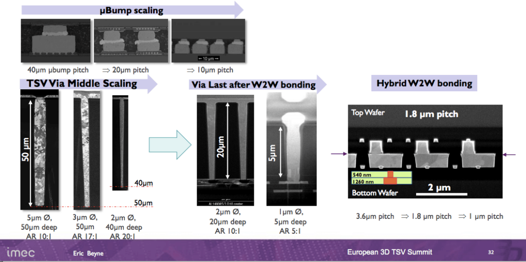
High performance computing has been the entry point for 3D TSV technologies, as it can bear the cost in exchange for the performance benefits. As this space is an unlikely candidate for FOWLP, researchers are continuing efforts in optimizing fine-pitch 3D technologies. Severine Cheramy, CEA-Leti, and Eric Beyne, imec, each talked about their respective progress. Cheramy focused on Leti’s research institute’s progress in fine-pitch 3D integration, and Beyne focused on scaling for 3D system integration. Both presentations discussed work being done in wafer-to-wafer and chip-to-wafer stacking. Beyne’s focus was on scaling the actual TSVs and bumps, and joints. He also talked about wafer-to-wafer hybrid bonding, and re-visited the concept of system partitioning. (Figure 1).

beynesummit

Figure 1: 3D interconnects. 3D SIC => 3D SoC. (Courtesy of imec)

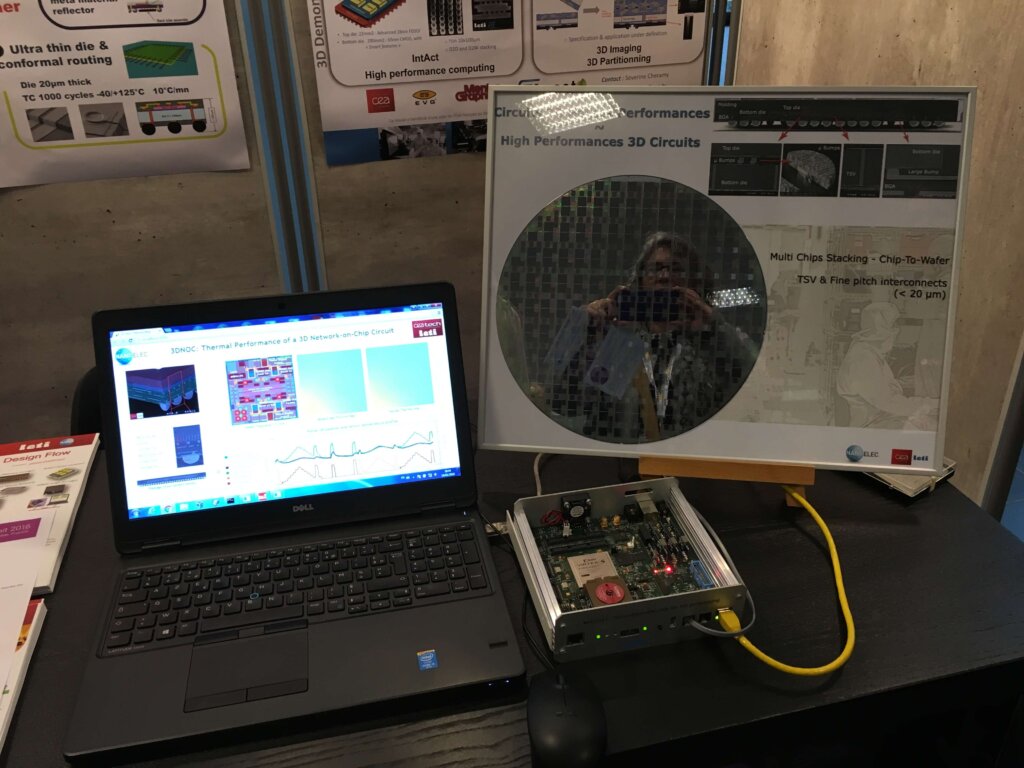
Cheramy stressed that interposer technology is a must for high performance/low power applications. Leti’s solution is to use chiplets on interposers that may or may not have memory integrated. The function of chiplets is performance. Die are partitioned into generic functional blocks that are easy to design and can be re-used application after application. She said the yield for the chiplets will be better in advanced nodes. (This sounds very similar to the work Subu Iyer has launched at UCLA, but he calls them dielets.) In July 2015, Leti introduced the 3D Network on Chip using the chiplet approach during SEMICON West. They had the demonstrator set up at their exhibit at the summit (Figure 2).

2016-01-18 16.44.38

Figure 2: Putting the 3D NoC through its paces.

Cheramy also provided an update on the IRT NanoElec 3D consortium, which EV Group and SET have recently joined to work on fine-pitch production processes. They are focused on developing highp-accuracy/high-speed chip-to-wafer direct bonding processes using self-assembly. High-aspect ratio vias are another area of focus for Leti. They are working together with SPTS and aveni on an alternative technology for TSV filling to meet aspect ratios >15:1.

There was a lot of representation from the FOWLP space, with market updates from TechSearch and Yole Développement, and presentations on specific technologies by Steffen Kroehnert, Nanium, Dave Hiner, Amkor, and Rama Alapati, GlobalFoundries, who focused on high density fan-out (HDFO). As I recently covered these at previous conferences, let me just summarize by saying that while conventional FOWLP (eWLB) has the potential to replace flip-chip chip-scale packages (FCCSP) and ball grid arrays (BGAs), HDFO challenges interposer-based technologies in performance and signal to noise ratios. The main difference between FOWLP and HDFO is the finer line/space requirements that HDFO can achieve due to different manufacturing processes. For example, eWLB starts with placing die face down on a molded wafer, and then performing the RDL. Amkor’s SWIFT and SLIM starts with the RDL layers on a sacrificial wafer, and then the die are attached and underfilled, followed by mold.

One newcomer to the 3D interconnect family presented at the 3D Summit was a process called 3D RDL, introduced by Ayad Ghannam, 3DIS Technologies, and targeting 3D system integration. Ghannam explained the concept of creating peripheral 3D interconnects using 3 lithography masks. He says this enables “native” 3D system integration without wire bond, TSV or PoP (Figure 3). Target applications for this technology are RF and mm-Wave applications, IoT and multi-chip applications, and MEMS and sensor packaging. Ghannam showed a number of interesting photos and diagrams. It reminded me a bit of the Vertical Circuits technology. The interconnect approach achieves 15/20µm L/S on a 120µm vertical step. As this is bigger than FOWLP’s 10µm l/s already in production, I don’t quite understand the advantages of this, or how to achieve high densities with this approach, but then again, I’m not an engineer. Still, it was interesting to see yet another new idea.

3D packaging

Figure 3: 3D RDL uses 3D lithography masks to create peripheral 3D interconnects. (Courtesy of 3DIS Technologies)

Even the printed circuit board (PCB) manufacturers want a piece of the advanced packaging action. We heard from Heinz Moitzi, AT&S AG, who explained the company’s laminate based embedded component technology (ECB). ECB uses the space in a printed circuit for active and/or passive components, which will be integrated in the core of the PCB core and connected by copper-plated micro vias. ECB is in production, says Moitzi, and it satisfies all the check-boxes: miniaturization, electrical performance, mechanical performance, thermal management, with added benefits of EMV shielding, supports modularization, low set-up costs, and offers and anti-tamper security element. Moitzi said ECP is being used in wearables, modules for wireless connections, medical products, Identification, and fan-out for fine pitch ICs. What I don’t understand is what makes this technology a 3D packaging approach?

The Target Products
Laurent Cargemmel, ATOS, talked about the company’s strategy for implementing 3D in its next-generation Bull Sequana supercomputer. He mentioned Xeon-EP, Xeon Phi, and Nvidia GPUs – Xeon Phi integrates Micron 3D memory stacks. He sees the advantages that the industry has been promoting, such as improved performance, reduced power, improved latency and bandwidth, and lower system cost.

Keynote speaker, Li Li, Cisco Systems, talked about how realizing the Internet of Everything relies on the next-generation of computing, network and storage systems, and that scaling alone is not the answer, as it is too costly. The key to success? You guessed it: 3D memory architectures and 3D packaging. While this is the story we’ve been telling for several years, its exciting to see that the customers are also in agreement.

After HPC, we heard from the image sensor sector, where TSVs are king. Jean-Luc Jaffard, Redbelt Consulting, gave a history lesson on image sensor technology, taking us through the evolution from 2D wire bond to 3D stacked backside illuminated (3D BSI) sensors in different varieties that implement TSVs. He said that all variations of BSI will become the standard imaging process. Jerome Chossat, ST Microelectronics, echoed that sentiment, and provided details on ST’s approach for 3D stacked image sensors for smart cameras. His talk focused on the wafer-to-wafer processes using a hybrid bonding approach (Figure 4).

3D Packaging

Figure 4: Comparison of BSI and 3D BSI. (Courtesy of ST Microelectronics)

One final presentation centered on products implementing 3D integration was by Martin Schrems, ams. His talk focused primarily on using 3D TSVs for IC sensor integration. He presented a smart system concept using an active interposer, TSVs, WLP and die-to-wafer assembly. Future products implementing these technologies are expected to include environmental and photonics sensors.

Now that 3D ball is finally rolling, it will be fun to watch it pick up steam. On January 19, the second day of the conference, Samsung Electronics announced it has put its second memory product implementing TSVs into production: the industry’s first 4-gigabyte (GB) DRAM package based on the second-generation (HBM2) interface, for use in high performance computing (HPC), advanced graphics and network systems, as well as enterprise servers. It will be interesting what difference a year makes when we gather again for the next European 3D Summit in Grenoble, January 23-25, 2017. Hope to see you there! ~ FvT


The post European 3D Summit: Putting 3D Packaging To Work appeared first on 3D InCites.


Success for 3D: What A Difference a Year Makes

$
0
0

During the 2015 European 3D TSV Summit, I drove attendees to distraction by asking each presenter what success looked like to them for 3D integration. The resulting responses became a blog post, What Does Success for 3D Integration Look Like? Now, a year later, I decided to revisit the topic by reminding last year’s presenters of their responses, and asking them for an update. As only few of the 2015 presenters presented at the 2015 European 3D Summit, I had to track down some of the responders. Some report great success, some moderate, and some have shifted focus of success to include fan-out wafer level packaging (FOWLP). Ampmg those I spoke with, here’s what they had to say:

  • Last year, Jan Vardaman, TechSearch International Inc, said:“Success is when I can go into a store and buy a product to tear down and find a 3D IC inside.” This year’s response: “Since AMD is shipping a product that has both a 3D IC with TSV stack and a silicon interposer, I would say the industry is successful in the commercialization of this technology. Cost and other factors limit some of the applications to high-performance, which makes unit volumes smaller. Sony is seeing success with its camera module using stacked image sensor and logic in mobile applications, but we will not see a memory and logic (application processor) stack in the mobile phone because of cost, business issues, thermal issues, and the fact that FOWLP offers almost the electrical performance benefit that could be provided by a memory and logic stack with TSVs.
  • In 2015, Rozalia Beica, Yole Développement defined success as entering volume production, and that overcoming the challenges so far was a step towards final success. So have we been successful? “I think so, yes,” she said. “We still have a ways to go to high volume production, but it seems end customers are seeing the advantages, and more and more products with 3D technologies are going into production.”
  • While Scott Jones, Alix Partners, didn’t present this year, last year he said “When I can go buy an iPad and it has 3D inside; when Intel and Samsung stands up here and says we have it, that’s what we see as success for this technology.” While no one from Intel or Samsung presented at this year’s summit, Samsung has gone into volume production with two memory stacks using 3D TSV technologies: their 3D TSV DDR4 and most recently, HBM2 DRAM. Additionally, Intel announced they will be implementing 2.5D and 3D technologies in 2016. Sounds like success to me.
  • For Eric Beyne, imec, last year, the most important thing for success would be adoption in to the market. As 2015 brought a number of 3D stacked memory products to the market, Beyne says, “We were right. It’s happened 100%.” So what’s next? “higher density wafer bonding is a bit further out in applications, but it’s coming.”
  • Last year, Farhang Yazdani, CEO Broadpak said success would be achieving a low cost secure system that is easy to integrate and is cost effective. So have we achieved this level of success? “I think we are there,” he said. “The price of silicon interposers has substantially been reduced, this is evident in the number of requests we have received.”
  • Georg Kimmich, ST Microelectronics, said last year that success for 3D was more about performance than cost, and was already successfully being implemented in image sensors. The next measure of success would be photonics. This year, he was happy to report that ST Microelectronics have built a photonics prototype, “so we’re getting there.” He added that in his opinion, FOWLP  is all hype just because Apple and TSMC are doing it. “It’s (FOWLP) only a replacement for PoP in smartphones and IoT applications, where the main concern is cost.,” he said.
  • Also on the topic of photonics development, Marco Fiorentino, HP Labs, defined success as a device that includes both the photonics and the TSV available from a foundry. He reported that they are not quite there yet, but hopes that work will continue in the coming year.
  • Last year David Butler, SPTS, said success would be when the OSATS are working in a similar direction, and not working on three or four technology types. Have we made progress? “I think we’re getting into that phase now, but perhaps not in the way we envisaged a couple of years ago. In 2016, the focus on TSV has softened, to be replaced by FOWLP with all OSATS and a number of foundries working hard to be ready for a fast ramp. Unlike TSV technology where the underlying concern was will it ever get into HVM, FOWLP ‎will go into significant volume in the 2nd half 2016 and continue on a fast growth right through 2020. It does feel like a technology whose time has come, both in terms of costs and of density. “
  • Martin Schrems, AMS, had said last year that if the forecasts held or exceeded predictions for use of 3D integration and wafer-level packaging, he will consider that success. The verdict? “In our case, its taken a longer time coming than many people thought,” he said. “The good news is, its coming now. Success is really around the corner. If you look closely. Its already happening.”
  • AMD’s Bryan Black defined success as when they got the first product out the door that was part of a product family, not just a “one-hit-wonder. Based on the interview I had with Black back in July,  I think we can safely say that by introducing the Fiji processor in its Radeon Fury product family, success has been achieved.
  • Ehrenfried Zschech, Fraunhofer IKTS said that the impression he gets from this year’s conference is that the variety of 3D solutions is increasing and simultaneously the number of materials integrated in 3D stacks which brings new challenges to reliability and particularly requires study of thermal mechanical stress induced effects.
  • On the supplier side, Hugo Pristauz, Besi, said last year that success would be when there are “no more headaches” with the die bond tool. Alignment accuracy and speed they’ve got covered, he said. “The tricky part is bond control.” After focusing on that for a year, he was happy to report that the bond control element is solved. While more challenges emerged, he says they have figured those out as well. “If I send my R&D guys to the customers, they can now achieve 100% yield.”
  • Last year, Markus Wimplinger, EV Group, had three measures of success: a stack with memory on logic in a smartphone, stacked memory in servers, and hybrid bonding in volume production for image sensor technology.  This year, he said that in terms of high-end applications, the memory stacks have appeared and that is a sign of success. “After hearing about all the efforts to optimize cost, we are on the road to success for the consumer products,” he added.
  • Last year, Amkor’s Ron Huemoeller equated success with return on investment. He was happy to report than in the 2.5D product area, the company has products in production and have met their goals. The goal for next year is to go into production with SWIFT, the company’s advanced, high density fan-out technology. He also had said that when people are willing to design into it with faith, that will be success. And to some extent, that has happened.
  • Saying that 3D IC is too expensive is not a good argument,”said Jürgen Wolf, Fraunhofer IZM, last year. “You could kill every good idea with this argument.” He predicted that reducing cost for TSVs and aligning technology specifications with the technology capabilities will bring 3D IC to success. He said he still believes this is true. Wolf says he sees potential for cost-efficent technology in production to accelerate integration into real products specifically for TSV. “It’s still important element in 3D integration,” he said.  He noted that we also have to align with assembly techniques and look at the integration of the whole package. As an example, he talked about work they are doing to develop thin, micro-bumped stacks that don’t require underfill. He said they are working with Ziptronix to eliminate underfill. Additionally, there needs to be more collaboration with product designer .

IMG_6250But the biggest question on my mind this year was, has anyone won the bet? Last year, Kevin Crofton, SPTS,  bet Thomas Leicht, Lam Research, that there would be at least one memory on logic stack in production in four years time. The Stake: the best bottle of wine Thomas Leicht has ever had, Chateau Patreus.

When I asked them the status of the bet, Crofton wanted to know if HBM used in the AMD Fiji processor counts, because it has four memory die stacked with TSVs on a logic die. I was willing to say yes, but this is a pretty good bottle of wine, and we don’t want to be cavalier about what constitutes memory on logic. So let’s put it to a vote below in the comment section. Does it count? Or does Crofton have 3 more years to win?  ~  F.v.T.


The post Success for 3D: What A Difference a Year Makes appeared first on 3D InCites.
From the Ashes of Moore’s Law: More than Moore Has Arrived

$
0
0

Now that the industry has finally called it a day for Moore’s law, will More than Moore be our guiding star for innovation?

Analysts have been predicting the demise of Moore’s law for about as long as I have been covering 3D integration technologies. During that time, Intel has steadfastly refused to succumb to that sentiment, and has continued to pursue ways to continue CMOS scaling. That’s understandable: Moore’s law was effectively a creation of Intel’s own Gordon Moore, so they weren’t going to go down easily, even though industry experts and researchers have been poking holes in traditional CMOS scaling — and essentially Moore’s law — for years as a way to validate the benefits of interposer and 3D integration technologies; also known as More than Moore technologies.

Morethanmoore

In the past few weeks since William Holt, Intel executive VP, spoke about Intel’s shift in focus at the International Solid State Circuits Conference (ISSCC) in San Francisco, January 31 – Feb 5, 2016, posts have rippled across semiconductor trade news, and science and technology blogs, declaring that Intel is finally ready to abandon it’s 51-year-old quest for doubling performance and speed every two years by doubling the number of transistors on a chip. Instead, focus is shifting to lower power consumption, even if that means sacrificing performance.

Several of bloggers quoted Holt as stating: “We’re going to see major transitions. The new technology will be fundamentally different. The best pure technology improvements we can make will bring improvements in power consumption but will reduce speed.” 

This version of Holt’s talk by Rick Merritt’s EE Times, makes it sound like Intel isn’t quite ready to let go of Moore’s law. Merritt quotes Holt as saying “The economics of Moore’s Law are sound if we focus on reducing cost per transistor.” However, Holt went on to say that the answer lies beyond CMOS scaling, and Intel will be launching research on “span tunneling FETs, ferroelectric FETs, spintronics, new III-V materials and more.” One of the key points is that while these new technologies improve power consumption, they do it at slower speeds, which kind of kills the main premise of Moore’s law.

In ExtremeTech, blogger Joel Hruska reports that Intel has acknowledged that the future of semiconductors may rely on technologies that reduce absolute performance in exchange for improved power consumption. He also noted that Intel’s motivation to shift focus away from pure performance improvements is because they are aggressively going after IoT applications, which calls for integration of disparate technologies in a small space, and that requires low power, and not spectacularly high performance. Additionally, Michael Grouthaus noted in a blog on Fast Company, that another reason it’s time to abandon Moore’s law has to do with our mobile computing habits. Faster chips have always meant more heat, which is easier to dissipate in a PC than in a tablet or smartphone.

Intel’s news has also reached the gaming community, which stands to lose from this news, as this is one space that is purely performance driven. In a post on Game Debate, a hot community for computer gamers, blogger “Joffy S” reports that the shift in focus towards energy efficiency, even at the expense of performance in the short-term, means “…we’re effectively capping out on CPU performance for now. If you buy a top-end CPU you can be confident it’s going to be gaming ready for a good long while.” He also predicted this would give AMD time to catch up.

They all must have missed the announcement by Babek Sabi, Intel corporate vice president and director of assembly and test technology development, that Intel would begin integrating 2.5D and 3D packaging technologies this year. This is how they will be able to improve performance and speed. We know it works, because AMD is already doing it for high performance gaming. Let me say this again, in case you weren’t listening: More than Moore technologies enable low power AND improved performance. In fact, Sabi said that achieving “really high-speed I/O” is not possible without multi-chip packaging.

Peter Bright posted a great blog on Arstechnica that details the rise and fall of Moore’s law, and why it’s time as a guide for what’s to come next is finally over. He doesn’t talk about Intel, but about the chip industry, and why its time to put Moore’s law behind us and look to other guides for innovation. Bright also cites an article in Nature, which announced that “The industry road map released next month will for the first time lay out a research and development plan that is not centered on Moore’s law. Instead, it will follow what might be called the More than Moore strategy: rather than making the chips better and letting the applications follow, it will start with applications — from smartphones and supercomputers to data centers in the cloud — and work downwards to see what chips are needed to support them.” I spoke about this a year ago with ITRS’s Bill Bottoms, who has been instrumental in bringing ITRS 2.0 into reality.

So did anyone from Intel actually say the words, “Moore’s law is Dead?”  Not that I can find, but many say that by announcing new technology development that will put power savings ahead of execution times, its pretty much the same thing. What we do know is that the rest of the industry is ready for the next star to guide us, and for those who have invested heavily in developing 3D integration technologies, this is good news. Because guess what? With 3D integration, you get both high performance and low power. And Intel finally figured that out. Long live More then Moore!  ~ FvT

The post From the Ashes of Moore’s Law: More than Moore Has Arrived appeared first on 3D InCites.
The HBM Supply Chain is Open for Business!

$
0
0

Last June, AMD made 3D integration history with its introduction of the Fiji gaming processor unit (GPU), which for the first time put high bandwidth memory (HBM) — a true 3D stack integrating memory die with through silicon via (TSVs) — into production. Fiji is a Si interposer-based module comprising an ASIC GPU surrounded by 4 HBM stacks, and it is powering AMD’s latest generation of Radeon Fury graphics cards for high-performance gaming. This event was a turning point for HBM, putting it ahead of Micron’s much-hyped Hybrid Memory Cube (HMC) as the go-to memory for high performance computing and networking applications. Since then, a number of companies have ramped their HBM programs into high gear and developed an HBM supply chain.

I was invited to emcee a seminar entitled, “Start your HBM/2.5D Design Today”, which took place on March 9 at the Computer History Museum in Mountain View, CA. It was a fitting venue for this event, as it represents the work of so many of the industry’s pioneers. The seminar featured presenters from five unique companies who have successfully developed an interposer-based HBM supply chain that has all the parts in place to ramp to volume production.

billIsaacson

Bill Isaacson, eSilicon, explains eSilicon’s role in the HBM Supply Chain. (photo credit: J. Patrick Corcoran, Cain Communication)

Kevin Tran, SK hynix; Paul Silvestri; Amkor Technologies; Bill Isaacson, eSilicon; Brian Daellenbach, Northwest Logic; and Chris Browy, Avery Design each described his company’s capabilities, and the role it plays in this supply chain. SK hynix provides the HBM stack. eSilicon is the ASIC vendor and system integrator. They work with the system architect to engineer the ASIC, and also design the interposer and package to deliver a turnkey solution. eSilicon also provides the HBM PHY and will own the yield for the final device. Northwest Logic provides the controller IP for the ASIC, Avery Designs provides the verification IP; specifically an HBM model used to verify the system. Amkor does the heavy lifting; integrating the HBM, interposer and ASIC wafers into a 2.5D assembly, and testing and shipping the module to the end customer. The message for the day: the HBM supply chain is open for business.

While I won’t dive into all the details of the presentations, here are some of the key take-aways:

  • Silvestri noted that TSVs should no longer be considered an R&D technology, but should be considered a production ready product. He noted that incoming interposer wafers from various sources demonstrate consistently good quality.
  • In response to the cost comparison of HBM vs. traditional DRAM, Silvestri said it’s difficult to cost-compare a package with basic memory vs. one with HBM. For example, in the case of the Fiji processor, they took memory traditionally placed “outboard” with wire-bond interconnects, vs. taking all the memory and stacking it on the interposer. Yes HBM adds cost to the package, but it’s the system-level cost needs to be considered.
  • Isaacson explained that cost analysis has shown that the HBM-based solution to increased bandwidth is considerably less expensive at system level, just in terms of ASIC real estate. To get the 2Tb/second of bandwidth that you get with a single HBM (12sq. mm) requires roughly 40 DDR4s (300sq mm). “If your object is increased bandwidth, than you win with HBM,” he said.

This fact is becoming very apparent to system architects.  Browy told me that in the past six months, the demand for HBM solution has “exploded.” Three years ago, noted Daellenbach, the hybrid memory cube (HMC) had the market lead on HBM as the memory solution for high performance computing and networking, and was expected to be the winner. But HBM has leapt ahead for a number of reasons: There are a number of sources because it’s a JEDEC standard. It’s also a lower power, and a lower cost solution than HMC. Reportedly, there have also been thermal issues with HMC due to the SERDES.

So how does this particular collaborative supply chain work? “HBM is the starting point, because they are looking for a solution to the bandwidth problem, and the ASIC isn’t the problem; it’s the memory that’s the problem,” said Tran. He said SK Hynix established the ecosystem along with eSilicon and invited the other companies to join in, because HBM is so complicated to adopt. “Unless we set up a supply chain with solutions that are ready, OEMs won’t be willing to invest,” he explained. While all the supply chain members recognize one another as the preferred vendor for their roles, it is an open supply chain, and customers are welcome to work with any or all of the companies. However, the benefit of working with the full supply chain is that they have invested in the R&D and have experience working with using this technology. According to Isaacson, they have built several test vehicles starting in 2011. He also showed two production designs for HPC and networking, one at 28nm and one at 14nm, that will ramp to volume this year.

If you missed the seminar, the group is hosting a webinar on March 29, 2016. It will be scheduled for two different times to accommodate time zones. Additionally. they will be publishing a white paper, which will be delivered to those who attended the seminar and register for the webinars. Look out for details coming soon.

The post The HBM Supply Chain is Open for Business! appeared first on 3D InCites.

System-in-Package was the Big Story at IMAPS DPC 2016

$
0
0

“The sum is greater than the whole of its parts.” ~ Aristotle (and Bill Chen)

While the technology tracks offered the latest developments in interposer and 3D IC processes, fan-out, wafer-level packaging, flip chip, MEMs, sensors and more, System-in-package (SiP) was the big story of the 2016 MAPS Device Packaging Conference, which was held March 15-17, 2016 in Fountain Hills, AZ. Why? Because SiP is the sum of all the advanced packaging parts, including interposer and 3D interconnects, and truly provides the value-add that advanced packaging now brings to semiconductor manufacturing.

There are many definitions of SiP, as we learned from the panelists on Tuesday evening’s SiP Panel, from Rozalia Beica, in her presentation during the Global Business Council, and from Bill Chen in his keynote on Fan-Out SiP:

• Rich Rice, ASE: SiP module is a package or module that contains a functional electronic system or subsystem that is integrated and miniaturized through IC assembly technologies.
• Lee Smith, UTAC: SiP involves heterogeneous integration of diverse functional parts into a standard package format (BGA, leadless, leadframe). It can include passives components and mixed assembly technologies.
• Rozalia Beica, Yole Développement: A SiP is two or more components with different functionalities packaged as a system or subsystem.
• Bob Lanzone, Amkor: we define advanced SiPs as multi-component, multi function products in an IC package. They require high-precision assembly technologies, which leverage Amkor’s strengths.
• Bill Chen, ASE: Heterogeneous Integration refers to the integration of separately manufactured components into a higher level assembly (SiP) that in the aggregate provides enhanced functionality and improved operating characteristics.

As Chen so eloquently noted in updating Gordon Moore’s vision for Moore’s Law:
“The future of integrated electronics is the future of electronics itself. The advantages of SiP through heterogeneous integration will bring about the proliferation of electronics, pushing this science into many new market application areas, internet of things, smart phones, cloud infrastructure, automotive and many other smart things.”

In her presentation, Hardware Opportunities in a Connected World, Jan Vardaman, Techsearch International Inc., detailed all the different connected devices across many markets beyond smartphones including wearables for healthcare, sports and fitness; automotive; and industrial automation. She also noted that smartphones, which are shipping at over 1B/year, are being used to control connected devices and so are still a very important part of the story.

Vardaman’s key message was that we are going to see connectivity everywhere with an increased use of sensors. The demand for lower cost solutions is driving adoption of new package designs. “There is no one single format, and no one-size-fits-all solution,” she said. “Economics and business considerations will drive package adoption. SiP is an enabler of many products for the trends in connectivity.”

Beica also talked about SiP; noting that it has evolved as a viable packaging methodology to support smart phone content, and has become the dominant package platform. She said growing and diversifying system requirements have continued to drive development of a variety of new package styles and configuration. SiP is used to integrate digital, RD, sensor, and mixed signal devices, with the advantages being small form factor, flexibility, the ability to integrate different technologies, higher performance, faster time-to-market, low cost, and added value. She added that a benefit of fan-out wafer level packaging (FOWLP) is the ability to incorporate more die and to form 3D SiPs. In his presentation, Bill Chen talked about a FO SiP test chip developed by ASE.

Rice noted that SiP is a subset of the module market; a market that is expected to grow from $53B in 2015 to $66B in 2016. As the OSATS, IDMs and EMS providers vie for market share, each is carving out its piece of the market. It seems the OSATS are each finding their niche and differentiators.

I asked the panelists what each of their company’s focus and strength is in this market.

At Intel, the focus and strength is on optimizing silicon in architectures to make new products feasible, and to do the advanced packaging required to make great things, explained Thomas DeBonis, Intel. Offering the IDM perspective, he pointed out important considerations such as who owns the yield when there are so many players involved in one SiP. Even starting with incoming die that sorted out well, it may be damaged in the dicing or assembly process. As SiPs move into highly integrated products this becomes a big challenge: who’s accountable for the loss? He says to be successful with new devices; business models need to be built around the yield risk.

Venkat Iyer, Flextronics, said the EMS provider’s focus is to provide “sketch-to-scale” modules, and as a system integrator, they handling everything from design to assembly, packaging and test. Their strength is in simple modules – they do not handle 2.5D or 3D IC. Iyer noted they are always met with resistance by suppliers to deliver known-good die (KGD), and that we would be amazed at the amount of in-process testing they do.

At UTAC, it’s about leveraging legacy packaging technology and embedded die technologies into a SiP module. Smith said the company doesn’t have a bumping line or do wafer level processing, and instead handles all the back-end assembly, with strength in test, leadless, and leadframe package types. They focus on power packages and thick leadframe technologies. Additionally, the recently joined forces with AT&S to develop a 3D SiP based on embedded die technology and provide an integrated supply chain for this unique SiP architecture. Smith also stressed the importance of test, and UTAC’s expertise in this area. “34% of our business is in test,” he said. “Test will be critical in modules and SiP.”

ASE Group is focused on module integration targeting the IoT/wearables market. Rice said the company’s strength is to leverage existing technologies and add new capabilities to the platforms to deliver cost-effective solutions in high volumes. ASE is able to tap into the synergies of its wholly owned subsidiary, contract manufacturer USI, and optain BOM components at a lower cost, while also having the right design tools and system design capabilities to do product design.

At Amkor, they have honed in on advanced SiP – targeting the high performance computing markets, networking, communications, mobile, automotive, and wearables. Lanzone says that HVM is both Amkor’s focus and its strength, as well as the ability to drive scale.

Essentially, SiP is broadly defined, and in all its forms, from leveraging legacy technologies to the most advanced interconnect processes, it is how we will integrate all sorts of functionality into all the electronics that we have come to rely on in our daily lives. ~ F.v.T.

The post System-in-Package was the Big Story at IMAPS DPC 2016 appeared first on 3D InCites.

EMIB, the 3D Technology Landscape, and other Keynote Moments from IMAPS DPC 2016

$
0
0

This year’s keynote talks at the 2016 IMAPS Device Packaging Conference (DPC 2016) provided some new insight into a number of interesting areas of importance to the advanced packaging community. I already addressed Bill Chen’s talk, which focused on system-in-package (SiP) and introduced a 3D Fan-out SiP approach. Here, I’ll focus on the key take-aways from the other three keynote talks that focused on Intel’s embedded multi-die interconnect bridge (EMIB) technology, imec’s 3D technology landscape, and Broadpak’s in-depth look at security issues with 2.5D and 3D technologies.

EMIB copy

Figure 1: Intel’s EMIB uses embedded Si “bridges” for high-density wiring.

Ravi Mahajan, Intel, kicked off this year’s even with a discussion about EMIB, which some classify as a fan-out wafer level technology (FOWLP), but seems to me to be an embedded die/interposer technology. Mahajan classified it as an on-silicon wiring approach that does not use through silicon vias (TSVs), but still provides improved bandwidth and density. He said traditional wire length for on-substrate wiring is up to 70mm. EMIB can achieve a similar length to Si interposer (~0.5mm to 10mm) through the use of embedded, thin silicon “bridges” that take the place of a full-size Si interposer. These are strategically located only in the few areas that high-density, multi-chip package connections are needed, rather than as a full-size Si interposer (Figure 1).

Because EMIB doesn’t require TSVs, a number of process steps are eliminated including TSV formation and fill, and TSV reveal and backside processes. Instead, the Si die are integrated into the package substrate, followed by typical 2.5D assembly. As such, in terms of overall cost, Mahajan says EMIB is better choice than Si interposer integration. Attendees posed questions about the reliability the CTE mismatch. Mahajan said he’s concerned about everything until it works; so far, EMIB works, and any CTE issues are manageable.

EMIB

FIgure 2: EMIB in the Altera Stratix 10 FPGA (Courtesy of Altera)

Mahajan also talked about the increasing demand for on-package CPU/memory bandwidth and capacity. Although Intel has integrated a version of the hybrid memory cube (HMC) into its Knight’s Landing Processor (he called it MC-DRAM), Mahajan said high bandwidth memory (HBM) has higher bandwidth than MC-CDRAM and is emerging as the memory-of-choice. While EMIB has not yet been used to package HBM, Mahajan says it is compatible with the technology, as it offers localized high-density interconnects to enable high bandwidth links. Currently, EMIB has been used to package Altera’s Stratix 10 FPGA.

imec’s 3D Technology Landscape

Gilbert Beyer, imec, followed Mahajan, and brought us up-to-date on some of the latest 3D integration technology advancements that are underway at imec.

Beyer began his talk by explaining why imec refers to the 3D technology landscape versus the 3D technology roadmap. “’Roadmap’ is very linear. For 3D, that’s clearly not the case. There are lots of options that coexist at the same time,” he explained.

imec has defined three main classes of 3D integration: 3D stacked IC (3D SIC), 3D system on chip (3D SOC) and 3D IC. Wiring and partitioning levels that require different process schemes, and achieve progressively smaller contact pitches differentiate them. 3D SiC requires global-level wiring, is partitioned at the die level and achieves pitches down to 5µm. 3D SOC has a range of wiring options including semi-global, intermediate, and local, and achieves pitches from 5µm down to 100nm at the local level. 3D SiC partitioning is achieved using die-to-wafer or die-to-interposer stacking. Depending on the partitioning level and pitch requirements, 3D SOC is achieved through wafer-to-wafer bonding in parallel, or through sequential processes using active layer bonding or deposition processes. 3D IC takes places at the transistor level, and uses active layer bonding or deposition processes in sequential processes.

Beyer focused the remainder of his talk on the latest technology advances to scale wafer bumping, and in wafer-to-wafer bonding. “We are confident that we can create smaller diameter TSVs,” he noted. “The concern is the die-to-die interconnect pitch. The state of µbump pitch is a significant mismatch with TSV interconnect density capability.”

While bumps have scaled successfully to 10µm, beyond that the challenges increase. Mechanical stability, alignment of the bonder, and bump slide-off are all issues. imec has been investigating a technique to embed µbumps in polymer. Cu damascene processes are used to realize the bumps, explained Beyer. While some questioned the cost of such a process, he said it doesn’t have to be more expensive because you perform passivation processes either way.

Beyer also talked about hybrid and dielectric bonding for wafer-to-wafer bonding schemes. While dielectric bonding doesn’t create an electrical connection between the two wafers, it is possible to introduce TSV via last after the wafers are bonded, achieving smaller diameter vias than with traditional TSV via last approaches.

Beyer’s concluding message is that 3D interconnect enables chip-to-chip connections for 3D SiC and 3D SOC. Scaling of key components of these technologies will enable higher interconnect densities; in particular TSVs, µbumps, and hybrid bonding. He also stressed that this is not an either/or situation. 3D interconnect technologies will co-exist, possibly even within the same system.

Securing SiPs

So as to not present a commercial for his company, Broadpak, Farhang Yazdani, focused his 3D keynote on security concerns we are facing due to the IoT rather than solutions; but rest assured, his company has solutions to the hardware security issues, in particular.

Any connected thing can be tampered with to carry out an action, noted Yazdani. For example, he cited the now-famous hacked Jeep, and also noted that an implanted medical device (IMD) can be un-secure, and can lead to catastrophic results if hacked.

Software assumes that the “core root of trust” is secure, but Yazdani says the reality is that it is not. Hardware security is a grave concern. “You might have developed a great product that is a great engineering achievement, but it’s a goldmine for intruders, and open to sniffing, spying, and tampering,” he said. An un-secure IoT SiP may not give you the right data; it may send data to other sources; it may perform tasks other than what it was intended for; or it may be activated or deactivated by adversaries. All of this can happen a number of ways: cyber attack through the network, through IP, through tampering with the chip, or a side-channel attack.

Hardware attacks, which are Broadpak’s focus for its advanced packaging solutions, can happen a number of ways. Cloning involves copying existing products and inserting malicious logic, idle channels, power and timing variations, test ports, tampering, and reverse-engineering so that you can probe the design and build your own. Overbuilding beyond the original PO is another way to do this. Design defects can be use to break into the device. Tampering allows for unauthorized access to the hardware through ‘back doors’.

Yazdani detailed the numerous points in the supply chain that pose potential security risks: On the design front, specs, tools and library models; IP development; and design-for-test (DFT) are all sensitive areas. Even more risky is during the manufacturing, and assembly processes; particularly front-end mask processes, wafer probe, packaging and test. The possibilities are somewhat mind-boggling.

For example, deleting or adding traces, or changing metallization can be done to introduce a Trojan. Additionally, changing the doping area changes the device functionality. Changing 128 bits to a random number of bits can reduce the security of a product.

Yazdani concluded his presentation by saying that Broadpak’s focus is on security, and that the company provides secure, tamper-resistant, anti-cloning technologies.

While this does nothing for the millions of un-secure devices already out in the world, at least going forward with new products,  we know that solutions are available. ~ FvT

The post EMIB, the 3D Technology Landscape, and other Keynote Moments from IMAPS DPC 2016 appeared first on 3D InCites.

Advanced Packaging and 3D come to MRS Spring Meeting

$
0
0

IMG_8683For the first time ever, the Materials Research Society (MRS) brought its annual Spring meeting to Phoenix. I have never attended this event, as it is deeply academic, and has not been on my radar for 3D or advanced packaging technologies. However, after finding out from fellow SemiSisters, Rozalia Beica, Yole Developpement, and Nancy Stoffel, GE Global Reseach, that there was an advanced packaging session for the first time ever: Materials Frontiers in Semiconductor Advanced Packaging, chaired by Stoffel and Jian Wei Dong, Dow Electronic Materials. There was also a paper on micro and nano computer tomography X-ray for 3D IC stacks delivered by Fraunhofer IPFTs’s Ehrenfried Zchech, I decided to pop in for the afternoon.

I ran into fellow technology journalist, Katherine Derbyshire, in the Advanced Packaging session. As an expert in thin-film manufacturing, Derbyshire has historically focused her coverage on front-end semiconductor technologies, so I was intrigued to find her in my queendom. She said it’s because advanced packaging is finally becoming a value-add to semiconductor manufacturing. I’ve noticed a lot more attention being paid to that topic on Semiconductor Engineering. I have to admit, I was feeling rather smug when she said that. As my entire semiconductor career has focused on advanced packaging and 3D integration, I’ve always been a believer. In any case, since I don’t have the scientific pedigree that Derbyshire has, I am really looking reading and sharing her post/s from this event.

Beica set the stage for the packaging session with a high-level presentation on the Future of Advanced Packaging. As this presentation was targeted to a new audience, she delivered a comprehensive view of the market evolution, packaging trends, computing trends, market drivers, and various package platforms with complete with product teardowns. One of the key takeaways from the materials perspective is that they need to serve a wide process window, as there is a broad range of packaging technologies from low, to mid and high range. Other key points included:

  • Flip-chip is still the dominant platform and will continue to grow, however, it could be significantly impacted by lower cost alternative platforms such as fan-out wafer level packages (FOWLP).
  • If Apple adopts TSMC InFO for its A10 APU processor in the iPhone 7 as predicted, then FOWLP could be a $2B business by 2020.
  • Fan-in is a mature technology, however, due to low cost and form factor, it is still a platform of interest in the industry.
  • 2.5D and 3DIC is already in production with CMOS image sensors, FPGAs, and MEMS. Most recently is the gaming processor unit (GPU) and high bandwidth memory (HBM) integration on an interposer.

I did not catch the remaining presentations in the session — which featured Georgia Tech’s developments in glass-based device and systems packaging as an alternative to CMOS scaling; one on sustainable material, from Purdue University; and presentations from TSMC and Hitachi Chemical on material challenges and technologies for wafer-based and stacking approaches —, because I wanted to catch Zchech’s presentation, scheduled simultaneously.

Zchech explained that when through-silicon vias (TSVs) are used as the method of interconnect in die stacking, the quality of the contacts (TSVs and solder bumps) is critical to performance. X-ray computer tomography (XCT) is a good characterization technique for obtaining information about these structures in a non-destructive way. However, current micro XCT are limited to detecting 1µm and above. Characterization in nanometer range below 100nm is performed using scanning electron microscopy (SEM) and transmission electron microscopy (TEM), both which require cross sections and are destructive methods. There is a gap between this neo-analysis and non-destructive testing that lies in the sub-micron space that Zchech says can be filled using sub-micron XCT. Not only that, but his team has built its own tool to do it.  He graciously contributed his abstract and presentation for publication on the 3D InCites Knowledge portal. You can read it here.  ~ FvT

The post Advanced Packaging and 3D come to MRS Spring Meeting appeared first on 3D InCites.
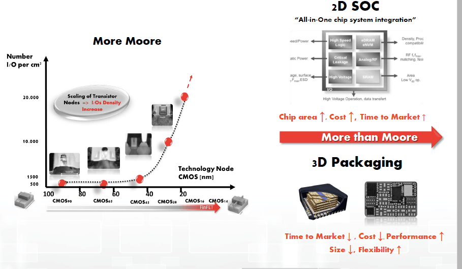
IPSO Challenge Update: The Smart Rock Bolt Success Story

$
0
0

Six months ago, I interviewed Jens Eliasson, associate professor at Luleå University of Technology (LTU), and co-developer of the Smart Rock Bolt, a vibration-sensor-based device used for instrumenting tunnels in mines to detect potential catastrophic collapses. He had just accepted the IPSO Challenge grand prize on behalf of his team. That story is here. I caught up with him after IoT World for an update. It turns out that winning the IPSO Challenge was quite a game changer for him. In his words, it “opened the floodgates” of opportunity.

smart rock bolt

Smart rock bolt case and electronics.

Eliasson says all the publicity on Reuters, the IPSO Alliance website, 3D InCites and others resulted in a number of inquiries from Swedish mining companies. It also led to entering a second contest run by the Swedish mining industry to support smaller companies and their ideas, and ultimately fund product development. He won that as well, and added €40K to the coffers to fund his company, ThingWave and started to actually manufacture Rock Bolt sensors and focus on real mining installations for a Swedish company, Boliden. Previously, field tests had been performed with the device. Every component had been tested in the lab or a mine, but a complete system had never been tested in a mine. “We are learning what works and what needs to be to be changed. By the beginning of next year, we plan to have a mine-tested working solution ready to go.” He added that there are teams working to improve the enclosure, which needs to be watertight if it is going to be in a mine for 5-10 years. They are also working on the software.

Shifting focus so rapidly from R&D to manufacturing has been somewhat of a wild ride, but Eliasson is enthusiastically embracing the challenge. “Most everything we see around us comes from mining activities, so the potential market is huge,” he explained. “Resources are finite, so we keep on digging deeper. The deeper we go, the higher the risk of collapse and the more we need to monitor and secure tunnels/mines.” Interest is primarily in using the Rock Bolt platform for a vibration sensor, but there is a huge potential for adding many other functionalities and opening this up to different markets. Other applications for the vibration sensor include seismic monitoring and ball bearing monitoring to perform condition marketing on rotating machinery and protect against damage. Additionally, other sensors, such as VOC, pressure, light and humidity, can be integrated to provide other capabilities.

While the focus is now on manufacturing the Rock Bolt system, Eliasson says there is still research to be done. In collaboration with Eistec, co-developer of the Rock Bolt, the team at ThingWave is developing software system on Eistec’s Mulle platform. They’ve also been able to outsource certain steps, such as the electronics.

Beyond winning the IPSO Challenge, Eliasson says complying with IPSO Standards has made it easier for third party companies to work with them because they can access more information from the system. Working with the companies within the IPSO Alliance has allowed him to establish credibility because they are all very important people in the industry. Additionally, being IPSO compliant means that new sensors added to the system are immediately identified and appear on the network.

“By winning IPSO Challenge, we got approval from IoT market,” said Eliasson. “From the mining award, we got approval from the mining industry. It’s been a really nice journey since December.”  ~ F.v.T


The post IPSO Challenge Update: The Smart Rock Bolt Success Story appeared first on 3D InCites.
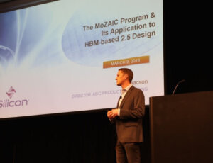

ECTC 2016: Memory Technology Advances and Prospects for Packaging

$
0
0

At ECTC 2016, which took place at the Cosmopolitan Las Vegas, Las Vegas, May 31-June 1, 2016, the special session entitled, Memory Technology Advances and Prospects for Packaging may have been one of the “most important starts to ECTC ever.” At least that was TechSearch’s, Jan Vardaman’s impression, and I can’t disagree, as it aptly set the tone for the week. Kudos to the session chair, Nanju Na, Xilinx, for lining up key industry experts from companies that have paved the way for 3D memory stacks and 2.5D integration: namely Bryan Black, AMD; Sandeep Bharathi, Xilinx; Nick Kim, SK hynix; Ravi Mahajan, Intel; and Craig Hampel, Rambus. Each presented updates on their company’s approaches to solving the memory bandwidth challenge through advanced packaging. Up first, Kim discussed Hynix memory package roadmap, noting that the company is leading new and advanced memory package development against the diverse and rapidly changing circumstances of the semiconductor industry. He offered some key takeaways:

Up first, Kim discussed Sk hynix’ memory package roadmap, noting that the company is leading new and advanced memory package development against the diverse and rapidly changing circumstances of the semiconductor industry. He offered some key takeaways:

  • Flip chip, wafer-level chip scale packaging (WLCSP), and stacking using through silicon vias (TSVs) are promising technologies that satisfy requirements for faster speed, wider bandwidth, and smaller, thinner packages.
  • TSVs are in mass production for DRAM.
  • 3D system-in-package (SiP) is suitable for placing memory next to logic, such as has been done on the Fiji processor introduced last year by AMD. sk Hynix provided the high bandwidth memory cube (HBM) for that product.
  • Fan-out wafer level (FOWLP) is a viable option for packaging memory, but cost reduction is needed. He specifically identified TSMC’s integrated fan-out (InFO) and Amkor’s silicon wafer integrated fan-out (SWIFT) as most promising options.
  • New process technologies being used for high-reliability and low-cost packaging include stealth dicing, and gold-free wire in wire bonding, such as aluminum or palladium Cu wire.

Mahajan talked about the trends of memory bandwidth, and that much like Moore’s Law, it doubles every 2.5 years. This has been consistent for over 15 years, he said. “Packaging needs to figure out how to handle this.” One way is to bring the memory closer to the CPU to improve power efficiency and performance. Speed and data trends call for wide and slow busses to lower power needs. He said a wide bus and on-package interconnect create power efficient interconnects between the CPU and memory.

Hempel veered in a different direction to talk about packaging memory from an architecture perspective. He queried when it comes to architecture and package design, which comes first? He explained how TSVs and 3D affect system architecture, noting that the three aspects that drive include capacity, power, and performance.

According to Hempel, using TSVs allows for a “master and slave” approach through the stack to improve density and capacity, which is critical for high-capacity data centers. He described the different ways to add capacity through 3D stacked DRAM:

  • Wide I/O uses the reduced length and parasitics of TSVs to reduce power.
  • HBM provides “near memory” for very high density interconnects on a simple logic layer.
  • The hybrid memory cube (HMC) differs architecturally. It provides advanced features in the logic layers including a high-speed link that allows for placement further than the CPU. It’s these differences in the functional logic layers that make HBM and HMC notably different.

For his part, Bryan Black, AMD mostly reprised his presentation from SEMICON West 2015, The Road to the AMD Fiji GPU, (and admitted as much in the beginning of his talk). I wrote about that here, but as is always the case with Black, he never REALLY gives the same talk twice. He made some especially profound statements in this version; as a silicon guy giving a nod to packaging: “15 years ago, I considered myself to be a “cowboy architect”, and didn’t have any interest in packaging. But then 15 minutes of learning about TSVs changed everything forever. Since then I’ve been fully focused on die stacking as an extension of Moore’s Law.” Black went on to say that he left Intel because it was clear “they were never, ever going to do die stacking.” That, of course, has changed, as evidenced by the work Mahajan is doing now.

Black also noted that by using HBM, they were able to deliver an enormous amount of bandwidth, only 60% of which is used by Fiji. This indicated to him that with HBM, we have rolled back the clock and have many years of performance scaling ahead of is before we run out of gas. In fact, Fiji is just the beginning. It’s all about co-design, he said. They are now working on a cost reduction and 3D usage model and are figuring out how to stack directly on top of the logic device.

The final speaker was Xilinx’ Bharathi, who talked about the company’s most recent first: 3D on 3D. Remember that Xilinx was the first to implement 2.5D interposer integration for FPGAs in its Virtex family (and won a 3D InCites award in the process). Now they have built a platform, christened UltraScale, which combines FinFET technologies, 3D IC structures, new memory, and multi-processing SoC (MPSoC) technologies to bring a higher level of integration into FPGAs. “FPGA is a system enabler,” explained Bharathi,“Memory technologies are evolving, and we need to support more SerDes bandwidth and compute bandwidth.” He added that packaging is a critical area to Xilinx. If you address packaging across the supply chain, you can reduce cost. The overall package spectrum requires industry support.

Jan Vardaman asked the question in many of our minds. Noting that while it’s clear TSVs have been widely adopted for memory in high-performance computing, could the panelists say when TSVs would be adopted into the top package in package-on-package (PoP) configurations, essentially bringing the large volumes the industry needs to support this technology. The answers were varied, but all tied to cost reductions.

Kim said currently, wire bonding meets the top package requirement in PoP, and so SK hynix doesn’t plan to change that “anytime soon.” Black was confident that the cost will come down. He reminded us that in 2011, the ASP for a Xilinx FPGA package was $17K. Thanks to AMD’s work, the cost of that package is now below $700. “The cost will keep going down. For a cell phone to adopt it, it has to be a commodity,” said Black. “We are a number of years away from it, but it will happen.”

Hempel concurred, calling it “trickle down technology.” What’s missing, he said is the business model of cooperation. Unlike the DRAM industry, integration is missing in mobile. As the economic benefit of TSV based DRAM is realized, more vendors will be able to negotiate that.

The key takeaway from this session was the fact that finally, and into the foreseeable future, advanced packaging technologies, and not scaling, are critical to reaching the capacity, power, and performance of today’s devices.


The post ECTC 2016: Memory Technology Advances and Prospects for Packaging appeared first on 3D InCites.
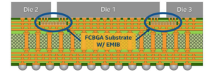
Words of Advice From Successful Women in Advanced Packaging

$
0
0

For the second consecutive year, Beth Keser, Qualcomm, organized and moderated the CMPT Woman’s Panel and Reception as part of ECTC’s special sessions. This year’s topic was titled, Maximize your Career Potential. Panelists included Jan Vardaman, founder, and president of TechSearch International, Inc; Rebeca Jimenez, SVP, Amkor Technology, Inc.; and Maryam Rofourgaran, former SVP of engineering at Broadcom and seasoned entrepreneur. Despite the title, the event was not exclusively for women, and it was a pleasant surprise once again to see the number of men who attended and took an interest in the topic.

The panelists shared their experiences of working and moving up the ladder of success to hold executive positions in a field that has historically been dominated by men, particularly at the executive level. They also offered tips on how to make that climb.

On their mentors and sponsors that led to success:

Vardaman said the support she received from various mentors has inspired her to “pay it forward” by offering internships to help young women get started. One area in particular that she provides guidance is in negotiating starting salaries. Her advice to women on this topic “Ask for 10K more than what they are offering. Women are being underpaid across many industries.”

Jimenez, who has a degree in electrical engineering, credits her older brother as her mentor and worked alongside him for 20 years of her career. What was the most significant thing she learned from him? “Always be humble. It’s about what you do, not what you say.” She also said that different managers through different jobs provided informal mentoring. “People who believed I could do what I didn’t know I could do. This has helped push me forward,” she said.

“As I’ve gone through different stages, my mentors have changed, as well as people who provided inspiration,” said Rofougaran. She includes Albert Einstein, Bill Gates, and Steve Jobs as role models. “They weren’t actually there to be mentors, but they motivated me a lot,” she said. “When I was in high school, I used to imagine myself getting a Nobel Prize.” More than anyone else, however, Rofougaran says her mother was her mentor, because of the way she raised her and her brother. “She taught us to be independent and believe in ourselves,” she said. “We grew up in Iran. She was always encouraging us and motivating us, saying there was nothing we couldn’t do.”

On their recommendations for young women who want to explore tech fields:
Noting that when she was young, women were not encouraged to go into engineering, so Vardaman said she didn’t see that as an option and got a degree in economics. “If you’re interested in sciences, find volunteer activities you can participate in and learn about your field of interest. There’s more available than there was 40 years ago,” she advised.

Jimenez noted that while girls perform better in math and science in middle school, they fall behind in high school because it’s not “cool to be a girl that’s good at math and science.”

Rofougaran agreed and added that it would help to capture girls’ interest if the programs were designed to be more interesting with a combination of games and drawing as part of how to learn coding and programming. Schools could help a lot by encouraging girls to go into science.

Keser recommended encouraging and enforcing an interest in the sciences. Once a month at Qualcomm, she said they offer young women the opportunity to learn some background knowledge with a female instructor to develop the skills needed to succeed in engineering in college. Why specifically women? “Boys have been doing these things all through their life. Girls haven’t been encouraged,” she explained, adding that there’s also a girls-only robotics team to even the playing field, and so the girls don’t have to compete with an aggressive boy to do all the work.

On how they handle career failures and setbacks:

“We learn from our successes; but we learn more from our failures because you analyze why you failed, try to learn from it, and move on,” said Jimenez.

Rofougaran pointed out that whoever else who took over that job could have failed too. “If you can learn from it, you’ll learn how to not fail the next time,” she said.

For her response, Vardaman shared an anecdote: When she turned in her resignation at MCC, where she served as international liaison, and told them she was going to start her own company, they tried to discourage her from doing that, and asked where she got the money to start her own company. “The made the assumption I would fail. So I worked extra hard, and when MCC eventually closed, I went in and bought all the scrap furniture.”

On what male leaders should do more or less of to help develop future female leaders:

Be encouraging, said Vardaman; not just to women, but for all young people. Stop to help young people get started and teach them the ropes of being successful.

Jimenez noted that all of her mentors were men. “They believed in me more than I believed in myself,” she said. She said men should encourage women to take responsibility for their jobs.

Keser recommended not promoting women too early just because they are women. Allow them to build technical competence for the first five or 10 years to lay the groundwork for the future.

Some final words of advice:
• Don’t wait to be promoted. Let your manager know what you want to do with your career.
• Network with other women. Take the time to go out to lunch and build relationships. It goes further than sitting in your cube to get work done.
• Volunteer in local CMPT events and develop contact outside your own company.
• Go outside your comfort zone. Opportunities will present themselves.

Thanks to Keser, for organizing this event, and to all the panelists, for sharing your experiences. You are insprirations to all, and I’m proud to call you my SemiSisters! ~ FvT

The post Words of Advice From Successful Women in Advanced Packaging appeared first on 3D InCites.

ECTC 2016: Is the Life after Moore’s Law?

$
0
0

Is Moore’s Law dead or not? It depends on your perspective. Last week at ECTC 2016, Rozalia Beica, Dow Electronic Materials, gathered a prestigious group of senior executives from the world’s leading microelectronics research institutes to discuss Life after Moore’s Law. Panelists included Marie-Noelle Semeria, CEA-Leti; Dim Lee Kwong, IME; Luc van den hove, imec; CP Wong, NCAP; and Subu Iyer, UCLA CHIPS. Each discussed the strategy they will pursue to continue innovations for next-generation computing technologies, with or without Moore’s Law. All but imec said efforts would be focused on packaging.

“Moore’s law has ended many times,” noted Semeria, “But we (CEA-Leti) are still alive, and the space for innovation is wider than ever.” She said that the real end of Moore’s Law began two years ago when we reached 28nm and the cost started to go up. But she said that the computing engine continues, and will reinvent itself into a “cognition engine” focused on function integration and energy efficiency.

Semeria described the roadmap for high-performance computing (HPC) as undergoing shifts in integration, technology, and architecture. At Leti, this has involved 3D integration comprising interposer-integrated chiplets with photonic links. By 2020, there will be a technology shift in memory materials including 3D VLSI and high-density 3D integrated Si photonic dies and neuromorphic materials for advanced chiplet architectures. Computer architecture will shift to quantum or neuromorphic architectures.

The Internet of Things (IoT) will feed HPC, because of the high rate of data we have to manage, noted Semeria, citing the latest trends in sensing, data fusion, connected health, artificial intelligence, deep learning, Big Data and cloud computing as evidence of this. “Knowledge will be key to handling the Data Economy,” she said.

Leti’s strategy is based on a system approach focused on miniaturization, connectivity, and security to support HPC, servers, µservers, connected health, etc. “Each application points to its moon,” noted Semeria, “It’s a broad space for innovation and requires a broad portfolio of technologies and skills to fix a solution.” Leti’s “moons” include photonics, advanced interposer, smart packaging, RF, and nanowires. Leti has achieved nanowires that are 3nm in diameter, which can play a role after 5nm.

Offering IME’s perspective and strategy, Kwong started out by noting that while IME has been benchmarking against imec and Leti for years, “I just met them tonight for the first time,” indicating Semeria and Van den hove. At IME, whatever the strategy, Kwong said they have to make sure the technology can be commercialized, as they are government-funded. He also talked about a paradigm shift to heterogeneous integration for system scaling. “Packaging has not scaled much in the last 40 years compared with transistors,” said Kwong. “Scaling the package will drive the next generation.” This includes fan-out, multi-die, and even the aforementioned neuromorphic chip.

IME’s strategy for solution-based IoT involves developing hardware and software integration for system design enablement. Kwong talked about IME’s Science Park 11, where they work on More-than-Moore technologies, and have a 300mm development line for 2.5D, 3D, and fan-out wafer level packaging (FLOWLP) processes. Additionally, Fusionopolis is a 300mm industry joint lab for advanced lithography, WLP, metrology, and more.

Wong and Iyer echoed the previous speakers sentiments that the future is about system integration using advanced packaging processes. Wong explained that this is the reason NCAP was formed in 2012, to bring advanced packaging to China. The center has established programs for 2.5D integration, fan-out wafer level system-in-package (FOWLSiP). This includes MEMS chips with through silicon vias (TSVs.)

With regard to CMOS scaling, Iyer is on the same page as Kwong. He says the biggest problem we have today in the hardware world is that Moore’s Law is an economic draw. Everything is based on cost-per-transistor. “If you can’t scale the chip, scale something else,” he said. “Nothing in the history of civilization has scaled so fast as silicon. But package and board features have scaled modestly. This is the focus of his work at UCLA – to scale the package. I have written previously about the CHIPS program Iyer launched in November at UCLA. To recap – the goal is to develop an app-like environment for hardware that can:

  • Cut time-to-market by 5-10x
  • Cut NRE cost by 10-20X
  • Allow extreme heterogeneity including extensions to cyber-physical systems
  • Develop a sophisticated manufacturing workforce

Since the launch, Iyer reports that they are in various stages of an agreement with 10 partners, and have received seed money from DARPA. SO they are well on their way to success in their first phase.

The only panelists waving the Moore’s Law Lives flag was Luc Van den hove, CEO imec. The institute is dedicated to extending Moore’s Law. “We believe that is the essence of what we have to do,” said Van den hove. He talked about meeting recently with Gordon Moore, and presenting him with a lifetime achievement award. “Yes, it becomes more difficult to get the same performance improvements from previous nodes. But there are solutions out there to extend Moore’s legacy,” he added. “Scaling not only will continue, it has to continue to keep momentum in this industry.”

He added that scaling will need a different approach. It will have to “morph” with added techniques to increase complexity. For example, there will be a transition from finFETs to horizontal nanowires, eventually to vertical nanowires, which will bring us to 3nm node or further, and “will keep us (imec) busy for the next decade.” It will require cost-effective technology enabled by EUV lithography. 2D will eventually slow down, and we will have to compensate by combining 2D with 3D technologies. He also talked about 3D heterogeneous integration, quantum computing, and cell stacking approaches like Crossbar and 3D NAND, all of which require innovation across the supply chain. “We have to bring together skill sets to push and extend Moore’s Law.”  That imec is focused on these technologies isn’t surprising, as their work is generally very early stage research and development at the concept stage. While they still work on optimizing 3D TSV processes for lower cost, the most exciting work has been already done.

What can the industry do to help these institutes reach their goals? Semeria called for the industry to accept its share of the roadmap. At the same time, researchers need to be more interested in solving industrial challenges. Van den hove seconded that, saying that companies higher up the food chain need to be more involved in new research. The industry also needs to take a longer-term view with regard to packaging, which has up until now been relegated to the bottom of the food chain. For at least the next few years, until new solutions to scaling can be figured out, packaging will clearly be in the driver’s seat. ~ F.v.T.


The post ECTC 2016: Is the Life after Moore’s Law? appeared first on 3D InCites.

Supplier Updates from ECTC 2016

$
0
0

In addition to attending the panel and plenary sessions at ECTC 2016, which took place May 31-June 3, 2016, I also spent a good deal of time talking to industry suppliers to get updates on their latest accomplishments that will impact the future of advanced semiconductor packaging, including interposer integration and 3D integration technologies.

Vincent Desmaris, Smoltek, told me all about the company’s molecular technology for growing nanostructures on substrates at temperatures below 390°C using chemical vapor deposition (CVD). “Temperature is critical so you don’t kill the component in the process,” explained Desmarais.

Although Smoltek’s processes were developed 10 years ago, achieving the low-temp aspect allows for nanostructure growth on an active device, making it possible to grow fine-pitch bumps directly on bond pads, or create on-chip capacitors.

Combined with interposer solutions, this also enables an energy storage solution that can be integrated with a sensor so it doesn’t need to rely on an external battery. This seems like a real breakthrough for the wearable device market.

Desmaris admitted that while CVD is a costly process, he thinks that front-end processes are beginning to be more accepted in the back-end. He’s provided some technical information that you can find here in the 3D InCites Knowledge Portal.

You might recall that at the 2014 IMAPS Device Packaging Conference, Kim Pollard, Dynaloy, presented results of ongoing feasibility studies for post-Bosch process residue removal using a solution with an improved environmental health and safety (EHS) profile. The goal was to develop a one-step process that removes both the photoresist polymer and the fluorine residue that remains on the via sidewall post-etch. The current method is a two-step process, in which the polymer is first removed using an oxygen plasma ash process. Then a wet process is used to remove the fluorine residue. Eliminating the ash step would provide considerable cost savings.

All went well in the first phase of the study done in Dynaloy’s labs on sample coupons, in which pre-screening showed fluorine was present, and subsequently removed with the new chemistry. However, in the second phase, which was performed using Dynaloy’s chemistry on full wafers in an SSEC wet wafer processing system, the wafers did not show any residual fluorine, so even though the wafers were clean at the end, conclusive data could not be provided. I wrote about it here.

Now, two years later, that conclusive data is available, thanks to the ongoing efforts of Pollard and Laura Mauer, CTO of Veeco Precision Surface Processing (formerly SSEC). The team compared the performance of Veeco’s wet process sequence in its WaferStorm platform with a more traditional process using oxygen ash, SC1 and HF clean. During the interactive poster session, Mauer reported that the combined chemistry and process not only cleans as well as the traditional approach, it eliminates the need for the ash step, reducing TSV RIE process time by 33%. This time, auger electron spectroscopy did show polymer and photoresist residue before cleaning. Electrical and physical analysis showed that the Veeco wet clean process removed both. Download the poster here.

At the KLA-Tencor booth, Pieter Vandewalle showed me several important developments with the ICOS T830 Component Inspector that targets the latest requirements for optical inspection of system-in-package (SiP) modules. First, he said as finer features are driving the industry to replace EMI shielding cap with metal coating spray, it’s critical to find exposed Cu defects in the shield coating to ensure the quality of the shield. This requires full-color inspection, which has been added to the tool. Inspection is performed right after sputtering to monitor the process and again after the functional test, explained Vandewalle. Additionally, he said there is a device cleaning feature consisting of a brushing system to remove burrs on the bottom of the EMI shield. The tool was selected for TSMC’s InFO process.

The next critical area for inspection is ball height for fan-out wafer level packages (FOWLP) in a package-on-package (PoP) configuration. The height of the total PoP stack is critical for smartphone manufacturers, and there is a tight tolerance on package height. For this, KLA-Tencor has added an entirely new module with a 3D measurement technique that measures with 5µm accuracy.

The last area Vandewalle touched on was the impact smaller nodes (14nm and below) is having on fan-in wafer level packaging. The use of low-k dielectrics is resulting in delamination and sidewall cracks because of the brittleness. To address this from an inspection perspective, KLA-Tencor will be introducing fast infrared inspections. Details were not available at this time.

IMG_0901IMG_0905In addition to these in-depth briefings, from a stroll through the technology corner I learned that:

Shinko has developed an organic interposer for 2.5D integration that reaches 2/2µm line and space feature sizes. Did you know that Shinko is not just a substrate supplier? It is a full-blown outsourced semiconductor assembly and test service (OSAT) provider (albeit a small one.)

Disco is partnering with Plasmatherm to develop plasma dicing technology.

Samtec, another packaging house that specializes in substrate selection, signal integrity, and design, has acquired nMode Solutions and its subsidiary, Triton Microtechnologies, Inc. If you recall, Triton has made a name for itself in the past few years for the development of glass interposer and through glass via (TGV) processes – something Samtec sees as an enhancement of its IC packaging capabilities that currently include wire bond, die attach, flip chip and underfill. This is their foray into the 2.5D world.

I’m sure this is just the tip of the proverbial iceberg of the latest innovations. With SEMICON West right around the corner, I’m looking forward to learning more from suppliers and will bring you all the latest on 3D InCites. Stay tuned! ~ FvT

The post Supplier Updates from ECTC 2016 appeared first on 3D InCites.

Executive Viewpoint: The New Advanced Packaging Landscape

$
0
0

Dongkai Shangguan 2016You might recall that a few year’s back (October 2013, to be precise), 3D InCites’ regular blogger, Paul Werbaneth, had the opportunity to interview Dongkai Shangguan, then CEO of the National Center for Advanced Packaging (NCAP) in Wuxi, China, which he helped found along with nine investors. They talked about lots of timely topics: the importance of industry-wide collaboration to bring down the costs of 2.5D/3D packaging technologies; Asia as a hotbed for growth in advanced packaging, (thus the establishment of NCAP); how optimizing and customizing semiconductor processing equipment for advanced packaging applications will help equipment cost/performance improvements; and a number of other things. (You can refresh your memory here)

A year ago, upon completion of his term at NCAP, Shangguan joined STATS ChipPAC as chief marketing officer. I caught up with him in Las Vegas at ECTC 2016 for an update on where he sees the advanced packaging landscape changing in this time of mergers and acquisitions, growth in China, and the slowing of scaling per Moore’s Law.

The Back Story
Shangguan joined STATS ChipPAC in the midst of its acquisition by Chinese semiconductor packaging conglomerate, JCET Group, comprising three companies each with its own management team. Jiangsu Changjiang Electronics Technology Co., Ltd. (JCET) is the largest outsourced semiconductor assembly and test service (OSAT) provider in China that mostly serves the Chinese market. Jiangyin Changdian Advanced Packaging Co., Ltd. (JCAP) provides wafer bump, probe and assembly, and STATS ChipPAC, headquartered in Singapore, rounds out the offering with a global manufacturing footprint and robust advanced packaging portfolio that includes wafer level packaging, flip chip and system-in-package (SiP) technology.

On The M&A Trends…
According to Research and Markets, 2015 was a record year for the total value of mergers and acquisition deals announced in the semiconductor industry, coming in at over $120B. The JCET acquisition of STATS ChipPAC was one such deal.

Consolidation is having an impact on the industry, and is a reflection of its maturity as a scaling economy, noted Shangguan. “Customers are getting bigger and demanding complete capabilities, services, and footprint. STATS ChipPAC and JCET are well positioned to sell bigger and larger,” he said. Together, he says the company will serve the semiconductor markets across North America, Europe, and Asia. “STATS ChipPAC has been strong in the North America and Europe,” he added. “With JCET’s strength in the Chinese market, we will be selling to customers all over the world and offering a broad portfolio from low-end, cost-sensitive products to high-end products.”

As a result of the acquisition, the JCET Group now has substantial manufacturing scale at various locations in China, including Jiangyin, Shanghai and Anhui, in addition to a sizeable manufacturing facility in Singapore which has significantly expanded its capacity recently, and a very large manufacturing operation in South Korea that is also currently going through a dramatic expansion. The Singapore factory focuses mainly on wafer level fan-in and fan-out technology, an area where there is growing demand in the market and the need for more capacity. The Korea operation, which was expanded and relocated to Incheon in 2014, is going through another considerable expansion to support growing demand for SiP solutions. “This is a new growth engine for us,” he said. “We continue to expand our SiP capabilities to support multiple market segments.”

On maturing FOWLP…
STATS ChipPAC was the earliest adopter of embedded wafer level ball grid array (eWLB), in production since 2009, and with 1B units shipped to date. Panel level processes, which will drive significantly better capital intensity and a lower unit cost for larger body sizes, are under development. “We are very strong and active in the fan-out space with mature processes. Yield is important and we have demonstrated very high yields with our fan-out process over the years. It takes time to build that through experience and expertise,” noted Shangguan.

On what’s driving the SiP and FOWLP markets…
“Packaging is a More than Moore solution; especially SiP,” noted Shangguan. “It’s an alternative path for system integration. SoC (system-on-chip) is one way, but SiP is a more flexible, cost-effective solution for system integration in many cases, particularly when heterogeneous technologies as involved.”

With the continued growth of the smartphone market and anticipated growth in sensor technologies for autonomous vehicles, the Internet of Things (IoT), wearable devices and more, they expect healthy growth for FOWLP and SiP. “SiP is everywhere,” he said. “There’s no doubt that the new advanced packaging landscape, including SiP and FOWLP, is changing the way semiconductor manufacturing does business. That’s why we have made the investment in capacity, floor space, and R&D.”

The post Executive Viewpoint: The New Advanced Packaging Landscape appeared first on 3D InCites.

Viewing all 256 articles
Browse latest View live